SCPS225E August 2011 – October 2024 TCA9509
PRODUCTION DATA
- 1
- 1 Features
- 2 Applications
- 3 Description
- 4 Pin Configuration and Functions
- 5 Specifications
- 6 Parameter Measurement Information
- 7 Detailed Description
- 8 Application and Implementation
- 9 Power Supply Recommendations
- 10Layout
- 11Device and Documentation Support
- 12Revision History
- 13Mechanical, Packaging, and Orderable Information
6 Parameter Measurement Information

| PIN | CL |
|---|---|
| SCLA, SDAA (A-side) | 50 pF |
| SDAB, SCLB (B-side) | 50 pF |

A. RT termination
resistance should be equal to ZOUT of pulse generators.
B. CL includes probe and
jig capacitance.
C. All input pulses are supplied by
generators having the following characteristics: PRR ≤ 10 MHz, ZO =
50 Ω, slew rate ≥ 1 V/ns.
D. The outputs are measured one at
a time, with one transition per measurement.
E. tPLH and
tPHL are the same as tpd.
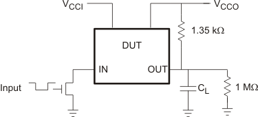
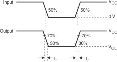
Figure 6-1 Test Circuit and Voltage
Waveforms