SCPS260C August 2017 – February 2022 TIC12400-Q1
PRODUCTION DATA
- 1 Features
- 2 Applications
- 3 Description
- 4 Revision History
- 5 Pin Configuration and Functions
- 6 Specifications
- 7 Parameter Measurement Information
-
8 Detailed Description
- 8.1 Overview
- 8.2 Functional Block Diagram
- 8.3
Feature Description
- 8.3.1 VS Pin
- 8.3.2 VDD Pin
- 8.3.3 Device Initialization
- 8.3.4 Device Trigger
- 8.3.5 Device Reset
- 8.3.6 VS Under-Voltage (UV) Condition
- 8.3.7 VS Over-Voltage (OV) Condition
- 8.3.8 Switch Inputs Settings
- 8.3.9 Interrupt Generation and INT Assertion
- 8.3.10 Temperature Monitor
- 8.3.11 Parity Check and Parity Generation
- 8.3.12 Cyclic Redundancy Check (CRC)
- 8.4 Device Functional Modes
- 8.5 Programming
- 8.6 Register Maps
- 8.7 Programming Guidelines
- 9 Application Information Disclaimer
- 10Power Supply Recommendations
- 11Layout
- 12Device and Documentation Support
- 13Mechanical, Packaging, and Orderable Information
8.4.3.4 Wetting Current Diagnostic
When the TIC12400-Q1 is used to monitor safety-critical switches, it may be valuable for the microcontroller to have knowledge of the operating status of the wetting current sources and sinks. This can be achieved by activating the wetting current diagnostic feature provided for inputs IN0 to IN3. IN0 and IN1 can be diagnosed for defective wetting current sources, while IN2 and IN3 can be diagnosed for defective current sinks.
The wetting current diagnostic feature can be activated by setting the WET_D_INx_EN bits in the CONFIG register to 1 for the desired inputs, where x can be 0, 1, 2, or 3. If activated, the TIC12400-Q1 checks the status of the wetting current sources and sinks for the configured input periodically as part of the polling sequence. If the wetting current is determined to be flawed, the TIC12400-Q1 pulls the INT pin low to notify the host and flag the WET_DIAG bit in the INT_STAT register to logic 1. The OI bit in the SPI flag is also asserted during SPI transactions. The microcontroller can then read bits IN0_D to IN3_D in register IN_STAT_MISC to learn more information on which wetting current source/sink is defective.
The wetting current diagnostic is not performed for inputs that are disabled (IN_EN_x bit = 0 in the IN_EN register) from polling, even if the feature is activated for those inputs. Also, it is critical to configure the current source/sink appropriately (CSO for IN0 and IN1, and CSI for IN2 and IN3) and program the input to ADC input mode before activating the wetting current diagnostic feature to prevent false interrupts from being generated. The wetting current diagnostic feature can be performed regardless of the states of external switches, and it is available in both continuous mode and polling mode.
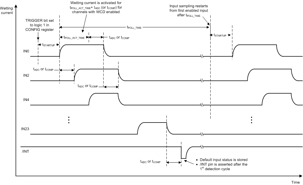
Figure 8-21 shows an example of the feature carried out in a typical polling sequence. In this example, it can be observed that the wetting current is activated for duration of tPOLL_ACT+ tADC for each input diagnosed (IN0 or IN2). Normal polling sequence resumes with IN4 and the wetting current is activated for tPOLL_ACT for the rest of the inputs. The diagnostic is not executed on inputs IN1 and IN3 in this example since they are disabled.
 Figure 8-21 An Example of the Polling Sequence in Standard Polling Mode With Wetting Current Diagnostic Enabled