SCPS268A September 2017 – February 2022 TIC10024-Q1
PRODUCTION DATA
- 1 Features
- 2 Applications
- 3 Description
- 4 Revision History
- 5 Pin Configuration and Functions
- 6 Specifications
- 7 Parameter Measurement Information
-
8 Detailed Description
- 8.1 Overview
- 8.2 Functional Block Diagram
- 8.3
Feature Description
- 8.3.1 VS Pin
- 8.3.2 VDD Pin
- 8.3.3 Device Initialization
- 8.3.4 Device Trigger
- 8.3.5 Device Reset
- 8.3.6 VS Under-Voltage (UV) Condition
- 8.3.7 VS Over-Voltage (OV) Condition
- 8.3.8 Switch Inputs Settings
- 8.3.9 Interrupt Generation and INT Assertion
- 8.3.10 Temperature Monitor
- 8.3.11 Parity Check And Parity Generation
- 8.3.12 Cyclic Redundancy Check (CRC)
- 8.4 Device Functional Modes
- 9 Programming
- 10Application and Implementation
- 11Power Supply Recommendations
- 12Layout
- 13Device and Documentation Support
- 14Mechanical, Packaging, and Orderable Information
8.3.9.3 Microcontroller Wake-Up
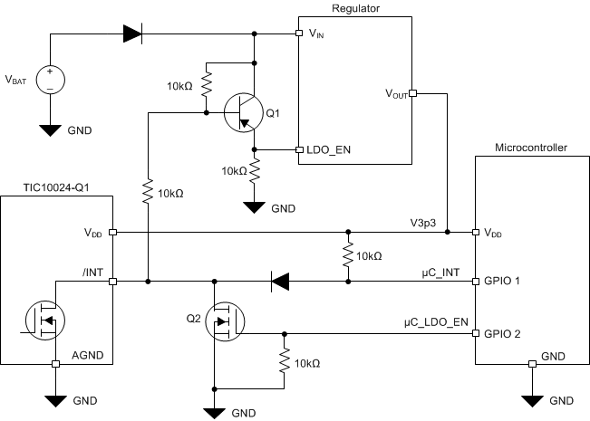
Using a few external components, the INT pin can be used for wake-up purpose to activate a voltage regulator through its inhibit inputs. An implementation example is shown in Figure 8-9. This implementation is especially useful for waking up a microcontroller in sleep mode to allow significant system-level power savings.
Before the wake-up event, the INT pin is in high impedance state on the TIC10024-Q1. The microcontroller can be kept in sleep state with all its GPIOs in logic low. Hence, Q2 remains off with its based in logic low state and the base of Q1 is weakly pulled-high to the VS level. This causes Q1 to remain off, and the LDO_EN signal is pulled-down to logic low to disable the regulator's output. VDD is therefore unavailable to both the TIC10024-Q1 device and the microcontroller and SPI communication is not supported. Switch status monitoring, however, is still active in the TIC10024-Q1.
When an event, such as switch status change, temperature warning, or overvoltage, occurs, the INT pin is asserted low by TIC10024-Q1, causing Q1 to turn on to activate the voltage regulator. The microcontroller is then reactivated, and the communication between the microcontroller and the TIC10024-Q1 is reestablished. The microcontroller can then access stored event information using SPI communication. Note since the INT pin is de-asserted after the INT_STAT register is read, the microcontroller is required to keep the regulator on by driving the μC_LDO_EN signal high. This allows VDD to stay high to provide power to the microcontroller and support SPI communications.
The wake-up implementation is applicable only when the device is configured to use the static INT assertion scheme.
 Figure 8-9 INT Connection to Support Microcontroller Wake-Up