SCPS268A September 2017 – February 2022 TIC10024-Q1
PRODUCTION DATA
- 1 Features
- 2 Applications
- 3 Description
- 4 Revision History
- 5 Pin Configuration and Functions
- 6 Specifications
- 7 Parameter Measurement Information
-
8 Detailed Description
- 8.1 Overview
- 8.2 Functional Block Diagram
- 8.3
Feature Description
- 8.3.1 VS Pin
- 8.3.2 VDD Pin
- 8.3.3 Device Initialization
- 8.3.4 Device Trigger
- 8.3.5 Device Reset
- 8.3.6 VS Under-Voltage (UV) Condition
- 8.3.7 VS Over-Voltage (OV) Condition
- 8.3.8 Switch Inputs Settings
- 8.3.9 Interrupt Generation and INT Assertion
- 8.3.10 Temperature Monitor
- 8.3.11 Parity Check And Parity Generation
- 8.3.12 Cyclic Redundancy Check (CRC)
- 8.4 Device Functional Modes
- 9 Programming
- 10Application and Implementation
- 11Power Supply Recommendations
- 12Layout
- 13Device and Documentation Support
- 14Mechanical, Packaging, and Orderable Information
8.3.8.3 Thresholds Adjustment
The threshold level for interrupt generation can be programmed by setting the THRES_COMP register. The threshold level settings can be set for each individual input groups and each group consists of 4 inputs. Four threshold levels are available: 2 V, 2.7 V, 3 V, and 4 V.
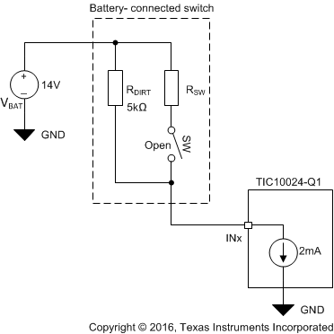
Remember to use caution when setting up the threshold for switches that are connected externally to the battery as there is a finite voltage drop (as high as VCSI_DROP_OPEN for 10mA and 15mA settings) across the current sinks. Therefore, even for an open switch, then voltage on the INx pin can be as high as VCSI_DROP_OPEN and the detection threshold shall be configured above it. It shall also be noted that a lower wetting current sink setting may not be strong enough to pull the INx pin close to ground in the presence of a leaky open external switch, as illustrated in the diagram below (see Figure 8-3). In this example, the external switch, although in the open state, has large leakage current and can be modelled as an equivalent resistor (RDIRT) of 5kΩ. The 2mA current sink is only able to pull the INx pin voltage down to 4 V, even if the switch is in the open state.
 Figure 8-3 Example Showing The Calculation of The INx Pin Voltage For A Leaky Battery-Connected Switch