SCPS275A July   2021  – December 2021 TCA9536

PRODUCTION DATA  

  1. Features
  2. Applications
  3. Description
  4. Revision History
  5. Pin Configuration and Functions
  6. Specifications
    1. 6.1 Absolute Maximum Ratings
    2. 6.2 ESD Ratings
    3. 6.3 Recommended Operating Conditions
    4. 6.4 Thermal Information
    5. 6.5 Electrical Characteristics
    6. 6.6 Timing Requirements
    7. 6.7 I2C Bus Timing Requirements
    8. 6.8 Switching Characteristics
    9. 6.9 Typical Characteristics
  7. Parameter Measurement Information
  8. Detailed Description
    1. 8.1 Overview
    2. 8.2 Functional Block Diagram
    3. 8.3 Feature Description
      1. 8.3.1 I/O Port
      2. 8.3.2 P3 or Interrupt (INT) Output
      3. 8.3.3 Pull-up Disable Functionality
    4. 8.4 Device Functional Modes
      1. 8.4.1 Power-On Reset
      2. 8.4.2 Powered-Up
    5. 8.5 Programming
      1. 8.5.1 I2C Interface
        1. 8.5.1.1 Writes
        2. 8.5.1.2 Reads
      2. 8.5.2 Software Reset Call
    6. 8.6 Register Maps
      1. 8.6.1 Device Address
      2. 8.6.2 Control Register and Command Byte
      3. 8.6.3 Register Descriptions
  9. Application Information Disclaimer
    1. 9.1 Application Information
    2. 9.2 Typical Application
      1. 9.2.1 Design Requirements
        1. 9.2.1.1 Minimizing ICC When I/Os Control LEDs
      2. 9.2.2 Detailed Design Procedure
      3. 9.2.3 Application Curves
  10. 10Power Supply Recommendations
    1. 10.1 Power-On Reset
  11. 11Layout
    1. 11.1 Layout Guidelines
    2. 11.2 Layout Example
  12. 12Device and Documentation Support
    1. 12.1 Documentation Support
      1. 12.1.1 Related Documentation
    2. 12.2 Receiving Notification of Documentation Updates
    3. 12.3 Support Resources
    4. 12.4 Trademarks
    5. 12.5 Electrostatic Discharge Caution
    6. 12.6 Glossary
  13. 13Mechanical, Packaging, and Orderable Information

Minimizing ICC When I/Os Control LEDs

When the I/Os are used to control LEDs, they are normally connected to VCC through a resistor as shown in Section 9.2. The LED acts as a diode so, when the LED is off, the I/O VIN is about 1.2 V less than VCC. The supply current, ICC, increases as VIN becomes lower than VCC.

Designs needing to minimize current consumption, such as battery power applications, should consider maintaining the I/O pins greater than or equal to VCC when the LED is off. Figure 9-2 shows a high-value resistor in parallel with the LED. Figure 9-3 shows VCC less than the LED supply voltage by at least 1.2 V. Both of these methods maintain the I/O VIN at or above VCC and prevent additional supply-current consumption when the LED is off.
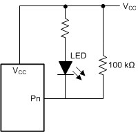
GUID-40A8982C-7564-4FE5-9203-D398375F9FAC-low.gifFigure 9-2 High-Value Resistor in Parallel with the LED
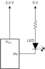
GUID-E6077475-A54F-47B6-9243-9230A350033B-low.gifFigure 9-3 Device Supplied by a Lower Voltage