SCPS275A July   2021  – December 2021 TCA9536

PRODUCTION DATA  

  1. Features
  2. Applications
  3. Description
  4. Revision History
  5. Pin Configuration and Functions
  6. Specifications
    1. 6.1 Absolute Maximum Ratings
    2. 6.2 ESD Ratings
    3. 6.3 Recommended Operating Conditions
    4. 6.4 Thermal Information
    5. 6.5 Electrical Characteristics
    6. 6.6 Timing Requirements
    7. 6.7 I2C Bus Timing Requirements
    8. 6.8 Switching Characteristics
    9. 6.9 Typical Characteristics
  7. Parameter Measurement Information
  8. Detailed Description
    1. 8.1 Overview
    2. 8.2 Functional Block Diagram
    3. 8.3 Feature Description
      1. 8.3.1 I/O Port
      2. 8.3.2 P3 or Interrupt (INT) Output
      3. 8.3.3 Pull-up Disable Functionality
    4. 8.4 Device Functional Modes
      1. 8.4.1 Power-On Reset
      2. 8.4.2 Powered-Up
    5. 8.5 Programming
      1. 8.5.1 I2C Interface
        1. 8.5.1.1 Writes
        2. 8.5.1.2 Reads
      2. 8.5.2 Software Reset Call
    6. 8.6 Register Maps
      1. 8.6.1 Device Address
      2. 8.6.2 Control Register and Command Byte
      3. 8.6.3 Register Descriptions
  9. Application Information Disclaimer
    1. 9.1 Application Information
    2. 9.2 Typical Application
      1. 9.2.1 Design Requirements
        1. 9.2.1.1 Minimizing ICC When I/Os Control LEDs
      2. 9.2.2 Detailed Design Procedure
      3. 9.2.3 Application Curves
  10. 10Power Supply Recommendations
    1. 10.1 Power-On Reset
  11. 11Layout
    1. 11.1 Layout Guidelines
    2. 11.2 Layout Example
  12. 12Device and Documentation Support
    1. 12.1 Documentation Support
      1. 12.1.1 Related Documentation
    2. 12.2 Receiving Notification of Documentation Updates
    3. 12.3 Support Resources
    4. 12.4 Trademarks
    5. 12.5 Electrostatic Discharge Caution
    6. 12.6 Glossary
  13. 13Mechanical, Packaging, and Orderable Information

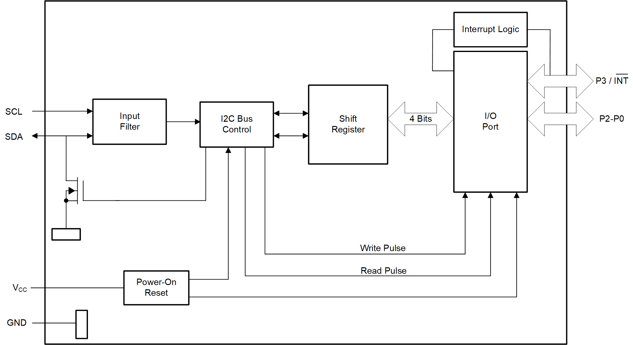
Functional Block Diagram

GUID-20210702-CA0I-V4P8-KXJK-TQXCS4CNJ870-low.gif Figure 8-1 Logic Diagram
Figure 8-2 Simplified Schematic Of P0 To P2
Figure 8-3 Simplified Schematic Of P3 / INT