SCPS308 October   2024 SN74AC164-Q1

PRODUCTION DATA  

  1.   1
  2. Features
  3. Applications
  4. Description
  5. Pin Configuration and Functions
  6. Specifications
    1. 5.1 Absolute Maximum Ratings
    2. 5.2 ESD Ratings
    3. 5.3 Recommended Operating Conditions
    4. 5.4 Thermal Information
    5. 5.5 Electrical Characteristics
    6. 5.6 Timing Characteristics
    7.     13
    8. 5.7 Switching Characteristics
    9. 5.8 Typical Characteristics
  7. Parameter Measurement Information
  8. Detailed Description
    1. 7.1 Overview
    2. 7.2 Functional Block Diagram
    3. 7.3 Feature Description
      1. 7.3.1 Balanced CMOS Push-Pull Outputs
      2. 7.3.2 Latching Logic
      3. 7.3.3 Standard CMOS Inputs
      4. 7.3.4 Wettable Flanks
      5. 7.3.5 Clamp Diode Structure
    4. 7.4 Device Functional Modes
  9. Application and Implementation
    1. 8.1 Application Information
    2. 8.2 Typical Application
      1. 8.2.1 Design Requirements
        1. 8.2.1.1 Power Considerations
        2. 8.2.1.2 Input Considerations
        3. 8.2.1.3 Output Considerations
        4. 8.2.1.4 Application Curve
    3. 8.3 Power Supply Recommendations
    4. 8.4 Layout
      1. 8.4.1 Layout Guidelines
      2. 8.4.2 Layout Example
  10. Device and Documentation Support
    1. 9.1 Documentation Support
      1. 9.1.1 Related Documentation
    2. 9.2 Receiving Notification of Documentation Updates
    3. 9.3 Support Resources
    4. 9.4 Trademarks
    5. 9.5 Electrostatic Discharge Caution
    6. 9.6 Glossary
  11. 10Revision History
  12. 11Mechanical, Packaging, and Orderable Information

Parameter Measurement Information

Phase relationships between waveforms were chosen arbitrarily for the examples listed in the following table. All input pulses are supplied by generators having the following characteristics: PRR ≤ 1MHz, ZO = 50Ω, tt < 2.5ns.

For clock inputs, fmax is measured when the input duty cycle is 50%.

The outputs are measured individually with one input transition per measurement.
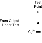
SN74AC164-Q1 Load Circuit for Push-Pull
                        Outputs
(1) CL includes probe and test-fixture capacitance.
Figure 6-1 Load Circuit for Push-Pull Outputs
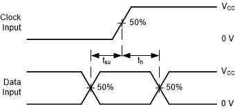
SN74AC164-Q1 Voltage Waveforms, Setup
                        and Hold TimesFigure 6-3 Voltage Waveforms, Setup and Hold Times
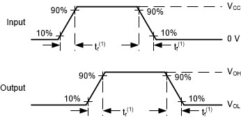
SN74AC164-Q1 Voltage Waveforms, Input
                        and Output Transition Times
(1) The greater between tr and tf is the same as tt.
Figure 6-5 Voltage Waveforms, Input and Output Transition Times
SN74AC164-Q1 Voltage Waveforms, Pulse
                        DurationFigure 6-2 Voltage Waveforms, Pulse Duration
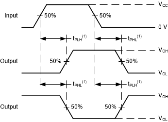
SN74AC164-Q1 Voltage Waveforms
                        Propagation Delays
(1) The greater between tPLH and tPHL is the same as tpd.
Figure 6-4 Voltage Waveforms Propagation Delays