SCPS308 October   2024 SN74AC164-Q1

PRODUCTION DATA  

  1.   1
  2. Features
  3. Applications
  4. Description
  5. Pin Configuration and Functions
  6. Specifications
    1. 5.1 Absolute Maximum Ratings
    2. 5.2 ESD Ratings
    3. 5.3 Recommended Operating Conditions
    4. 5.4 Thermal Information
    5. 5.5 Electrical Characteristics
    6. 5.6 Timing Characteristics
    7.     13
    8. 5.7 Switching Characteristics
    9. 5.8 Typical Characteristics
  7. Parameter Measurement Information
  8. Detailed Description
    1. 7.1 Overview
    2. 7.2 Functional Block Diagram
    3. 7.3 Feature Description
      1. 7.3.1 Balanced CMOS Push-Pull Outputs
      2. 7.3.2 Latching Logic
      3. 7.3.3 Standard CMOS Inputs
      4. 7.3.4 Wettable Flanks
      5. 7.3.5 Clamp Diode Structure
    4. 7.4 Device Functional Modes
  9. Application and Implementation
    1. 8.1 Application Information
    2. 8.2 Typical Application
      1. 8.2.1 Design Requirements
        1. 8.2.1.1 Power Considerations
        2. 8.2.1.2 Input Considerations
        3. 8.2.1.3 Output Considerations
        4. 8.2.1.4 Application Curve
    3. 8.3 Power Supply Recommendations
    4. 8.4 Layout
      1. 8.4.1 Layout Guidelines
      2. 8.4.2 Layout Example
  10. Device and Documentation Support
    1. 9.1 Documentation Support
      1. 9.1.1 Related Documentation
    2. 9.2 Receiving Notification of Documentation Updates
    3. 9.3 Support Resources
    4. 9.4 Trademarks
    5. 9.5 Electrostatic Discharge Caution
    6. 9.6 Glossary
  11. 10Revision History
  12. 11Mechanical, Packaging, and Orderable Information

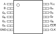
Pin Configuration and Functions

SN74AC164-Q1 PW
                                                  Package,14-Pin
                                                  TSSOP (Top
                                                  View)Figure 4-1 PW Package,
14-Pin TSSOP
(Top View)
SN74AC164-Q1 WBQA Package14-Pin
                                                  WQFN (Top
                                                  View)Figure 4-2 WBQA Package
14-Pin WQFN
(Top View)
Table 4-1 Pin Functions
PIN TYPE(1) DESCRIPTION
NAME NO.
A 1 I Gated serial input A
B 2 I Gated serial input B
QA 3 O Parallel output A
QB 4 O Parallel output B
QC 5 O Parallel output C
QD 6 O Parallel output D
GND 7 G Ground
CLK 8 I Clock input, rising edge triggered
CLR 9 I Asynchronous register clear input, active low
QE 10 O Parallel output E
QF 11 O Parallel output F
QG 12 O Parallel output G
QH 13 O Parallel output H
VCC 14 P Positive supply
Thermal pad(2) The thermal pad can be connect to GND or left floating. Do not connect to any other signal or supply.
Signal Types: I = Input, O = Output, P = Power, G = Ground.
WBQA package only.