SFFS011 February 2023 TPS560430-Q1
4 Pin Failure Mode Analysis (Pin FMA)
This section provides a Failure Mode Analysis (FMA) for the pins of the TPS560430-Q1. The failure modes covered in this document include the typical pin-by-pin failure scenarios:
- Pin short-circuited to Ground (see Table 4-2)
- Pin open-circuited (see Table 4-3)
- Pin short-circuited to an adjacent pin (see Table 4-4)
- Pin short-circuited to VIN (see Table 4-5)
Table 4-2 through Table 4-5 also indicate how these pin conditions can affect the device as per the failure effects classification in Table 4-1.
| Class | Failure Effects |
|---|---|
| A | Potential device damage that affects functionality |
| B | No device damage, but loss of functionality |
| C | No device damage, but performance degradation |
| D | No device damage, no impact to functionality or performance |
Following are the assumptions of use and the device configuration assumed for the pin FMA in this section:
- Device used within the 'Recommended Operating Conditions' and the 'Absolute Maximum Ratings' found in the appropriate device data sheet.
- Configuration as shown in the 'Example Application Circuit' found in the appropriate device data sheet.
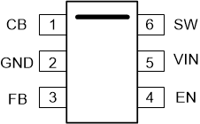
Figure 4-1 shows the TPS560430-Q1 pin diagram for the SOT-23-6 package. For a detailed description of the device pins please refer to the 'Pin Configuration and Functions' section in the appropriate device data sheet.
 Figure 4-1 Pin
Diagram
Figure 4-1 Pin
Diagram| Pin Name | Pin No. | Description of Potential Failure Effect(s) | Failure Effect Class |
|---|---|---|---|
| CB | 1 | No output voltage | B |
| GND | 2 | Normal Operation | D |
| FB | 3 | The regulator will operate at maximum duty cycle. Output voltage will rise to nearly the input voltage (VIN) level. Possible damage to customer load and/or output stage components may occur. No effect on device. | B |
| EN | 4 | Loss of ENABLE functionality Device will remain in shutdown mode. | B |
| VIN | 5 | Device will not operate. No output voltage will be generated. Output capacitors will discharge through input short. Large reverse current may damage device. | A |
| SW | 6 | Damage to internal FET. | A |
| Pin Name | Pin No. | Description of Potential Failure Effect(s) | Failure Effect Class |
|---|---|---|---|
| CB | 1 | No output voltage | B |
| GND | 2 | VOUT can be abnormal due to switching noise on analog circuits. | B |
| FB | 3 | VOUT will be higher than programmed output voltage. | B |
| EN | 4 | Loss of ENABLE functionality. Erratic operation; probable loss of regulation. | B |
| VIN | 5 | No output voltage | B |
| SW | 6 | No output voltage | B |
| Pin Name | Pin No. | Shorted to | Description of Potential Failure Effect(s) | Failure Effect Class |
|---|---|---|---|---|
| CB | 1 | GND | No output voltage | B |
| GND | 2 | FB | The regulator will operate at maximum duty cycle. Output voltage will rise to nearly the input voltage (VIN) level. Possible damage to customer load and/or output stage components can occur. No effect on device. | B |
| FB | 3 | GND | The regulator will operate at maximum duty cycle. Output voltage will rise to nearly the input voltage (VIN) level. Possible damage to customer load and/or output stage components can occur. No effect on device. | B |
| EN | 4 | VIN | No damage to device. Loss of ENABLE functionality. | B |
| VIN | 5 | SW | Damage to internal FET | A |
| SW | 6 | VIN | Damage to internal FET | A |
| Pin Name | Pin No. | Description of Potential Failure Effect(s) | Failure Effect Class |
|---|---|---|---|
| CB | 1 | No output voltage. CBOOT ESD clamp will run current to destruction. | A |
| GND | 2 | No output voltage. Damage to other pins referred to GND. | A |
| FB | 3 | If VIN exceeds 16 V, damage will occur. No output voltage. | A |
| EN | 4 | No damage to device. Loss of ENABLE functionality. | B |
| VIN | 5 | No effect | D |
| SW | 6 | internal FET | A |