SFFS755 November 2023 SN74HCS14-Q1
4.1 BQA, D, DYY, and PW Packages
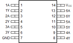
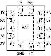
Figure 4-2 shows the SN74HCS14-Q1 pin diagram for the BQA, D, DYY, and PW packages. For a detailed description of the device pins and their corresponding pin type, please refer to the Pin Configuration and Functions section in the SN74HCS14-Q1 data sheet. Thermal Thermal Pad should be tied directly to GND plane to avoid potential failures that can cause excessive current.
 Figure 4-1 Pin Diagram (D, DYY, and
PW) Packages
 Figure 4-2 Pin Diagram (BQA)
Package
Figure 4-2 Pin Diagram (BQA)
PackageTable 4-2 Pin FMA for Device Pins
Short-Circuited to Ground
| Pin Name | Pin No. | Description of Potential Failure Effect(s) | Failure Effect Class |
|---|---|---|---|
| A | 1, 3, 5, 9, 11, 13 | Input pin is forced to the low logic state. See Device Function Table in the device data sheet for details of how the failure affects functionality. | B |
| GND | 7 | Normal operation. | D |
| Y | 2, 4, 6, 8, 10, 12 | Can cause excessive output current; output remains in the low output state independent of input states. | A |
| VCC | 14 | Device is not powered. System level damage can occur in this scenario. | B |
|
Thermal Pad(1) |
— | Normal operation. | D |
(1) BQA package only
Table 4-3 Pin FMA for Device Pins
Open-Circuited
| Pin Name | Pin No. | Description of Potential Failure Effect(s) | Failure Effect Class |
|---|---|---|---|
| A | 1, 3, 5, 9, 11, 13 | Pin is floating, can change output state and cause excessive current from VCC to GND. See Implications of Slow or Floating CMOS Inputs. | A |
| GND | 7 | Device is not powered. | B |
| Y | 2, 4, 6, 8, 10, 12 | Normal operation. | D |
| VCC | 14 | Device is not powered. | B |
|
Thermal Pad(1) |
— | Normal operation. |
D |
(1) BQA package only
Table 4-4 Pin FMA for Device Pins
Short-Circuited to Adjacent Pin
| Pin Name | Pin No. | Shorted to | Description of Potential Failure Effect(s) | Failure Effect Class |
|---|---|---|---|---|
| A | 1, 3, 5, 9, 11, 13 | A | Two inputs shorted together can cause a loss of functionality or damage to the device. Damage to the device can occur when the input voltage (VI) is driven such that VIL < VI < VIH. | A |
| A | 1, 3, 5, 9, 11, 13 | Y | Can cause loss of functionality or damage to the device. Damage to the device can occur due to feedback oscillation causing excessive current consumption. | A |
| A | 1, 3, 5, 9, 11, 13 | GND | Input pin is forced to the low logic state. See Device Function Table in the device data sheet for details of how the failure affects functionality. | B |
| A | 1, 3, 5, 9, 11, 13 | Thermal Pad | Input pin is forced to the low logic state. See Device Function Table in the device data sheet for details of how the failure affects functionality. |
B |
| A | 1, 3, 5, 9, 11, 13 | VCC | Input pin is forced to the high logic state. See Device Function Table in the device data sheet for details of how the failure affects functionality. | B |
| Y | 2, 4, 6, 8, 10, 12 | GND | Can cause excessive output current; output remains in the low output state independent of input states. | A |
| Y | 2, 4, 6, 8, 10, 12 | Thermal Pad | Can cause excessive output current; output remains in the low output state independent of input states. |
A |
| Y | 2, 4, 6, 8, 10, 12 | VCC | Can cause excessive output current; output remains in the high output state independent of input states. | A |
Table 4-5 Pin FMA for Device Pins
Short-Circuited to
VCC
| Pin Name | Pin No. | Description of Potential Failure Effect(s) | Failure Effect Class |
|---|---|---|---|
| A | 1, 3, 5, 9, 11, 13 | Input pin is forced to the high logic state. See Device Function Table in the device data sheet for details of how the failure affects functionality. | B |
| GND | 7 | Device can not be powered because short is external to device. System level damage can occur in this scenario. | B |
| Y | 2, 4, 6, 8, 10, 12 | Can cause excessive output current; output remains in the high output state independent of input states. | A |
| VCC | 14 | Normal operation. | D |
| Thermal Pad(1) | — | Device is not powered. System level damage can occur in this scenario. |
B |
(1) BQA package only