SFFS767 March 2024 TPS3808E
4 Pin Failure Mode Analysis (Pin FMA)
This section provides a Failure Mode Analysis (FMA) for the pins of the TPS3808E. The failure modes covered in this document include the typical pin-by-pin failure scenarios:
- Pin short-circuited to Ground (see Table 4-2)
- Pin open-circuited (see Table 4-3)
- Pin short-circuited to an adjacent pin (see Table 4-4)
- Pin short-circuited to supply (see Table 4-5)
Table 4-2 through Table 4-5 also indicate how these pin conditions can affect the device as per the failure effects classification in Table 4-1.
| Class | Failure Effects |
|---|---|
| A | Potential device damage that affects functionality |
| B | No device damage, but loss of functionality |
| C | No device damage, but performance degradation |
| D | No device damage, no impact to functionality or performance |
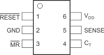
Table 4-1 shows the TPS3808E pin diagram. For a detailed description of the device pins please refer to TPS3760-Q1 in the Pin Configuration and Functions section of the data sheet.
 Figure 4-1 Pin Diagram DYY Package14-Pin SOT-23
Following are the assumptions of use and the device configuration assumed for the pin FMA in this section:
- At VDD (MIN) ≤ VDD ≤ VDD (MAX)
- MR = Open, CT = Open,
- Output reset Pullup Resistor (RPULLUP) = 10kΩ, Output reset pullup voltage (VPULLUP = 3.5V
-
Sense is monitoring VDD
- Typical values are at TA = 25°C, VDD = 3.5V, CVDD=0.1µF, and VIT = 3.3V unless stated otherwise.
| PIN NAME | PIN NO. | DESCRIPTION OF POTENTIAL FAILURE EFFECT(S) | FAILURE EFFECT CLASS |
|---|---|---|---|
| RESET | 1 | Forces RESET to be held low. | B |
GND | 2 | No damage to device. No impact to functionality. | D |
| MR | 3 | RESET will be asserted. | B |
CT | 4 | RESET is latched low if an undervoltage condition occurs. | B |
SENSE | 5 | RESET will be asserted. | B |
VDD | 6 | VDD short to GND, Device has no power for normal operation | B |
| PIN NAME | PIN NO. | DESCRIPTION OF POTENTIAL FAILURE EFFECT(S) | FAILURE EFFECT CLASS |
|---|---|---|---|
| RESET | 1 | Reset functionality will be lost since it's not being pulled up to VDD. | B |
GND | 2 | Device is unpowered. | B |
MR | 3 | Normal operation. | D |
CT | 4 | Normal operation. | D |
SENSE | 5 | No damage to the device. Reset is asserted. | B |
VDD | 6 | Device is unpowered. | B |
| PIN NAME | PIN NO. | SHORTED TO | DESCRIPTION OF POTENTIAL FAILURE EFFECT(S) | FAILURE EFFECT CLASS |
|---|---|---|---|---|
|
RESET |
1 |
GND |
Forces RESET to be held low. |
B |
|
GND |
2 |
/MR |
RESET will be asserted. |
B |
|
MR |
3 | CT |
RESET is latched low if an undervoltage condition occurs. |
B |
|
CT |
4 | SENSE |
RESET is latched low if an undervoltage condition occurs. |
B |
|
SENSE |
5 |
VDD |
Normal operation. |
D |
|
VDD |
6 |
/RESET |
Large current can flow into RESET when in error condition. This can cause permanent damage. |
A |
| PIN NAME | PIN NO. | DESCRIPTION OF POTENTIAL FAILURE EFFECT(S) | FAILURE EFFECT CLASS |
|---|---|---|---|
| RESET | 1 | Large current can flow into RESET when in error condition. This can cause permanent damage. | A |
GND | 2 | Device has no power for normal operation | B |
| MR | 3 | Normal operation. | D |
CT | 4 | RESET is latched low if an undervoltage condition occurs. | B |
SENSE | 5 | Normal operation. | D |
VDD | 6 | Normal operation. | D |