SFFS786 February 2024 TXU0204-Q1
4 Pin Failure Mode Analysis (Pin FMA)
This section provides a Failure Mode Analysis (FMA) for the pins of the TXU0204-Q1 (TSSOP-14 and VQFN-14 package). The failure modes covered in this document include the typical pin-by-pin failure scenarios:
- Pin short-circuited to Ground (see Table 4-2)
- Pin open-circuited (see Table 4-3)
- Pin short-circuited to an adjacent pin (see Table 4-4)
- Pin short-circuited to supply (see Table 4-5 and Table 4-6)
Table 4-2 through Table 4-6 also indicate how these pin conditions can affect the device as per the failure effects classification in Table 4-1.
| Class | Failure Effects |
|---|---|
| A | Potential device damage that affects functionality |
| B | No device damage, but loss of functionality |
| C | No device damage, but performance degradation |
| D | No device damage, no impact to functionality or performance |
Following are the assumptions of use and the device configuration assumed for the pin FMA in this section:
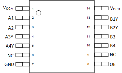
Figure 4-1 shows the TXU0204-Q1 pin diagram for the TSSOP-14 packages. For a detailed description of the device pins please refer to the Pin Configuration and Functions section in the TXU0204-Q1 data sheet.
 Figure 4-1 Pin Diagram (TSSOP-14) Package
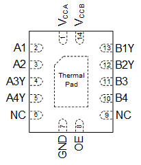
Figure 4-2 shows the TXU0204-Q1 pin diagram for the VQFN-14 package. For a detailed description of the device pins please refer to the Pin Configuration and Functions section in the TXU0204-Q1 data sheet.
 Figure 4-2 Pin Diagram (VQFN-14 Package)
| Pin Name | Pin No. | Description of Potential Failure Effect(s) | Failure Effect Class |
|---|---|---|---|
| VCCA | 1 | Device will not be powered or damaged, because short is external to device. System level damage may occur in this scenario. | B |
| A1 | 2 | Ax will be LOW, if corresponding Bx is HIGH, there will be potential damage to the device if the current is not limited. If corresponding Bx is LOW, then nothing will occur, no damage. | B |
| A2 | 3 | B | |
| A3Y | 4 | B | |
| A4Y | 5 | B | |
| NC | 6 | Normal operation. | D |
| GND | 7 | Normal operation. | D |
| OE | 8 | All I/Os will be fixed into high impedance (tri-state). | B |
| NC | 9 | Normal operation. | D |
| B4 | 10 | Bx will be LOW, if corresponding Ax is HIGH, there will be potential damage to the device if the current is not limited. If corresponding Ax is LOW, then nothing will occur, no damage. | B |
| B3 | 11 | B | |
| B2Y | 12 | B | |
| B1Y | 13 | B | |
| VCCB | 14 | Device will not be powered or damaged, because short is external to device. System level damage may occur in this scenario. | B |
| Pin Name | Pin No. | Description of Potential Failure Effect(s) | Failure Effect Class |
|---|---|---|---|
| VCCA | 1 | Device will not be powered. | B |
| A1 | 2 | Ax input pins will be grounded internally. Ax output pins will be in HiZ if device is disabled. If device is enabled, it will be HIGH or LOW depending on the input. | D |
| A2 | 3 | D | |
| A3Y | 4 | D | |
| A4Y | 5 | D | |
| NC | 6 | Normal operation. | D |
| GND | 7 | Device will not be powered. | B |
| OE | 8 | I/Os may be high impedance or active, unknown input state. | A |
| NC | 9 | Normal operation. | D |
| B4 | 10 | Bx input pins will be grounded internally. Bx output pins will be in HiZ if device is disabled. If device is enabled, it will be HIGH or LOW depending on the input. | D |
| B3 | 11 | D | |
| B2Y | 12 | D | |
| B1Y | 13 | D | |
| VCCB | 14 | Device will not be powered. | B |
| Pin Name | Pin No. | Shorted to | Description of Potential Failure Effect(s) | Failure Effect Class |
|---|---|---|---|---|
| VCCA | 1 | A1 | Ax will be HIGH, if corresponding Bx is LOW, there will be potential damage to the device if the current is not limited. If corresponding Bx is HIGH, then nothing will occur, no damage. | B |
| A1 | 2 | A2 | Two inputs shorted together will not cause damage unless there is external bus contention that drives the input such that VIL < Input Voltage < VIH in which case excessive supply current to GND may cause damage. Two outputs shorted together or an input shorted to an output may cause damage if there is external bus contention that drives one LOW while driving the other HIGH. | A |
| A2 | 3 | A3Y | A | |
| A3Y | 4 | A4Y | A | |
| A4Y | 5 | NC | Normal operation. | D |
| NC | 6 | GND | Normal operation. | D |
| GND | 7 | OE | All I/Os will be fixed into high impedance (tri-state). | B |
| OE | 8 | NC | Normal operation. | D |
| NC | 9 | B4 | Normal operation. | D |
| B4 | 10 | B3 | Two inputs shorted together will not cause damage unless there is external bus contention that drives the input such that VIL < Input Voltage < VIH in which case excessive supply current to GND may cause damage. Two outputs shorted together or an input shorted to an output may cause damage if there is external bus contention that drives one LOW while driving the other HIGH. |
A |
| B3 | 11 | B2Y | A | |
| B2Y | 12 | B1Y | A | |
| B1Y | 13 | VCCB | Bx will be high, if corresponding Ax is low, there will be potential damage to the device if the current is not limited. If corresponding Ax is high, then nothing will occur, no damage. | B |
| VCCB | 14 | VCCA | Device will not be powered or damaged, because short is external to device System level damage may occur in this scenario. | B |
| Pin Name | Pin No. | Description of Potential Failure Effect(s) | Failure Effect Class |
|---|---|---|---|
| VCCA | 1 | Normal operation. | D |
| A1 | 2 | Ax will be HIGH, if corresponding Bx is LOW, there will be potential damage to the device if the current is not limited. If corresponding Bx is HIGH, then nothing will occur, no damage. | B |
| A2 | 3 | B | |
| A3Y | 4 | B | |
| A4Y | 5 | B | |
| NC | 6 | Normal operation. | D |
| GND | 7 | Device will not be powered or damaged, because short is external to device. System level damage may occur in this scenario. | B |
| OE | 8 | All I/Os will be active, device cannot be disabled. | B |
| NC | 9 | Normal operation. | D |
| B4 | 10 | Bx will be HIGH, if corresponding Ax is LOW, there will be potential damage to the device if the current is not limited. If corresponding Ax is HIGH, then nothing will occur, no damage. | B |
| B3 | 11 | B | |
| B2Y | 12 | B | |
| B1Y | 13 | B | |
| VCCB | 14 | Device will not be powered or damaged, because short is external to device. System level damage may occur in this scenario. | B |
| Pin Name | Pin No. | Description of Potential Failure Effect(s) | Failure Effect Class |
|---|---|---|---|
| VCCA | 1 | Device will not be powered or damaged, because short is external to device. System level damage may occur in this scenario. | B |
| A1 | 2 | Ax will be HIGH, if corresponding Bx is LOW, there will be potential damage to the device if the current is not limited. If corresponding Bx is HIGH, then nothing will occur, no damage. | B |
| A2 | 3 | B | |
| A3Y | 4 | B | |
| A4Y | 5 | B | |
| NC | 6 | Normal operation. | D |
| GND | 7 | Device will not be powered or damaged, because short is external to device. System level damage may occur in this scenario. | B |
| OE | 8 | All I/Os will be active, device cannot be disabled. | B |
| NC | 9 | Normal operation. | D |
| B4 | 10 | Bx will be HIGH, if corresponding Ax is LOW, there will be potential damage to the device if the current is not limited. If corresponding Ax is HIGH, then nothing will occur, no damage. | B |
| B3 | 11 | B | |
| B2Y | 12 | B | |
| B1Y | 13 | B | |
| VCCB | 14 | Normal operation. | D |