SFFS832 September 2024 UCC27301A-Q1 , UCC27311A-Q1
4.1 SOIC Package
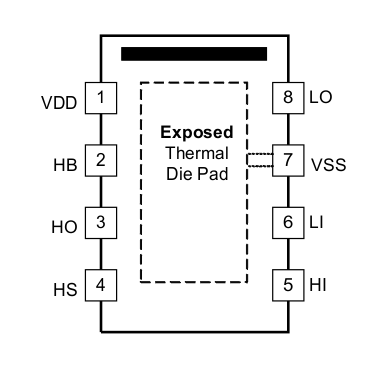
Figure 4-1 shows the UCC27311A-Q1 pin diagram for the SOIC package. For a detailed description of the device pins, see the Pin Configuration and Functions section in the UCC27311A-Q1 data sheet.
 Figure 4-1 Pin Diagram (SOIC) Package
Table 4-2 Pin FMA for Device Pins
Short-Circuited to Ground
| Pin Name | Pin No. | Description of Potential Failure Effects | Failure Effect Class |
|---|---|---|---|
| VDD | 1 | No power is applied to the device. HO and LO are in a low state. | B |
| HB | 2 | HO and LO are in unknown state. | A |
| HO | 3 | HO and LO are in unknown state. | A |
| HS | 4 | HO and LO are in unknown state. | A |
| HI | 5 | HO is in a low state. | B |
| LI | 6 | LO is in a low state. | B |
| VSS | 7 | No impact. | D |
| LO | 8 | HO and LO are in unknown state. | A |
Table 4-3 Pin FMA for Device Pins
Open-Circuited
| Pin Name | Pin No. | Description of Potential Failure Effects | Failure Effect Class |
|---|---|---|---|
| VDD | 1 | No power is applied to the device. HO and LO are in a low state. | B |
| HB | 2 | HO is pulled to HS potential. | B |
| HO | 3 | HO is disconnected from the system. | B |
| HS | 4 | HO is pulled to HB potential. | B |
| HI | 5 | HO is in a low state. | B |
| LI | 6 | LO is in a low state. | B |
| VSS | 7 | HO is in a low state. LO is pulled to VDD. | B |
| LO | 8 | HO is disconnected from the system. | B |
Table 4-4 Pin FMA for Device Pins
Short-Circuited to Adjacent Pin
| Pin Name | Pin No. | Shorted to | Description of Potential Failure Effects | Failure Effect Class |
|---|---|---|---|---|
| VDD | 1 | HB | HO and LO are in unknown state. | A |
| HB | 2 | HO | HO is in unknown state. | A |
| HO | 3 | HS | HO is in unknown state. | A |
| HS | 4 | N/A | N/A | D |
| HI | 5 | LI | LO and HO follows the logic truth table per the data sheet. The input states depends on the system. | B |
| LI | 6 | VSS | LO is in a low state. | B |
| VSS | 7 | LO | LO is in unknown state. | A |
| LO | 8 | N/A | N/A | D |
Table 4-5 Pin FMA for Device Pins Short-Circuited to
Supply
| Pin Name | Pin No. | Description of Potential Failure Effects | Failure Effect Class |
|---|---|---|---|
| VDD | 1 | N/A | D |
| HB | 2 | HO and LO are in unknown state. | A |
| HO | 3 | HO and LO are in unknown state. | A |
| HS | 4 | HO and LO are in unknown state. | A |
| HI | 5 | HO and LO follow the logic truth table per the data sheet with LI stuck in a high state. | B |
| LI | 6 | HO and LO follow the logic truth table per the data sheet with LI stuck in a high state. | B |
| VSS | 7 | HO is in a low state. LO is pulled to VDD. | B |
| LO | 8 | HO and LO are in unknown state. | A |