SFFSA06 December 2024 TCAN1472-Q1
4 Pin Failure Mode Analysis (Pin FMA)
This section provides a failure mode analysis (FMA) for the pins of the TCAN1472-Q1 and TCAN1472V-Q1. The failure modes covered in this document include the typical pin-by-pin failure scenarios:
- Pin short-circuited to ground (see Table 4-2)
- Pin open-circuited (see Table 4-3)
- Pin short-circuited to an adjacent pin (see Table 4-4)
- Pin short-circuited to VCC (see Table 4-5)
- Pin short-circuited to VBAT (see Table 4-6)
- Pin short-circuited to VIO (Table 4-7)
Table 4-2 through Table 4-7 also indicate how these pin conditions can affect the device as per the failure effects classification in Table 4-1.
| Class | Failure Effects |
|---|---|
| A | Potential device damage that affects functionality. |
| B | No device damage, but loss of functionality. |
| C | No device damage, but performance degradation. |
| D | No device damage, no impact to functionality or performance. |
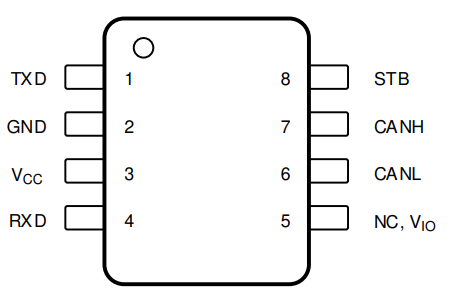
Figure 4-1 shows the TCAN1472-Q1 and TCAN1472V-Q1 SOIC (D) pin diagram.
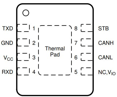
Figure 4-2 shows the TCAN1472-Q1 and TCAN1472V-Q1 VSON (DRB) pin diagram.
Figure 4-3 shows the TCAN1472-Q1 and TCAN1472V-Q1 SOT (DDF) pin diagram.
For a detailed description of the device pins please refer to the Pin Configuration and Functions section in the TCAN1472-Q1 and TCAN1472V-Q1 data sheets.
 Figure 4-1 SOIC (D) Pin Diagram
 Figure 4-3 SOT (DDF) Pin Diagram
 Figure 4-2 VSON
(DRB) Pin Diagram
Figure 4-2 VSON
(DRB) Pin DiagramFollowing are the assumptions of use and the device configuration assumed for the pin FMA in this section:
- VCC = 4.5V to 5.5V
- VBAT = 6V to 24V
- VIO = 1.7V to 5.5V
| Pin Name | Pin No. | Description of Potential Failure Effects | Failure Effect Class |
|---|---|---|---|
| TXD | 1 | Device enters dominant time out mode. Unable to transmit data. | B |
| GND | 2 | None. | D |
| VCC | 3 | Device not powered, high ICC current. | B |
| RXD | 4 | RXD default is high-side FET ON, with pin short-to-ground, forms direct path between supply and ground causing high current. | A |
| NC | 5 | None. | D |
| VIO | 5 | Device is in protected mode. Transceiver is passive on bus. | B |
| CANL | 6 | VO(REC) specification violated. Degraded EMC performance. | C |
| CANH | 7 | Device cannot drive dominant to the bus, no communication is possible. | B |
| STB | 8 | STB stuck low, transceiver unable to enter low-power mode. | B |
| Thermal Pad | - | None. | D |
| Pin Name | Pin No. | Description of Potential Failure Effects | Failure Effect Class |
|---|---|---|---|
| TXD | 1 | TXD pin defaults high, device always recessive and unable to transmit data. | B |
| GND | 2 | Device not powered. | B |
| VCC | 3 | Device not powered. | B |
| RXD | 4 | No RXD output, unable to receive data. | B |
| NC | 5 | None. | D |
| VIO | 5 | Device is in protected mode. Transceiver passive on bus. | B |
| CANL | 6 | Device cannot drive dominant on the bus, unable to communicate. | B |
| CANH | 7 | Device cannot drive dominant on the bus, unable to communicate. | B |
| STB | 8 | STB pin defaults high, transceiver stuck in low-power mode. | B |
| Thermal Pad | - | None. | D |
| Pin Name | Pin No. | Shorted to | Description of Potential Failure Effects | Failure Effect Class |
|---|---|---|---|---|
| TXD | 1 | GND | Device enters dominant time out mode. Unable to transmit data. | B |
| GND | 2 | VCC | Device not powered, high ICCcurrent. | B |
| VCC | 3 | RXD | RXD output stuck high, unable to receive data. | B |
| NC | 5 | CANL | None. | D |
| VIO | 5 | CANL | Bus stuck recessive, no communication is possible. IOS current can be reached on CANL. | B |
| CANL | 6 | CANH | Bus stuck recessive, no communication is possible. IOS current can be reached on CANH/CANL. | B |
| CANH | 7 | STB | Driver and receiver turn off when a dominant is driven. Not entering normal mode is possible. | B |
| Pin Name | Pin No. | Description of Potential Failure Effects | Failure Effect Class |
|---|---|---|---|
| TXD | 1 | TXD stuck high, unable to transmit data. | B |
| GND | 2 | Device not powered, high ICC current. | B |
| VCC | 3 | None. | D |
| RXD | 4 | RXD pin stuck high, unable to receive data. | B |
| NC | 5 | None. | D |
| VIO | 5 | IO pins operate as 5V input and outputs. Microcontroller can be damaged if VCC > VIO. | C |
| CANL | 6 | RXD always recessive, no communication is possible. IOS current can be reached. | B |
| CANH | 7 | VO(REC) specification violated, degraded EMC performance. | C |
| STB | 8 | STB stuck high, transceiver always in standby mode. | B |
| Pin Name | Pin No. | Description of Potential Failure Effects | Failure Effect Class |
|---|---|---|---|
| TXD | 1 | Absolute maximum violation, transceiver can be damaged. Unable to transmit data. | A |
| GND | 2 | Device not powered, high IBAT current. | B |
| VCC | 3 | Absolute maximum violation, transceiver can be damaged. Bus can be unable to communicate. | A |
| RXD | 4 | Absolute maximum violation, transceiver can be damaged. Unable to receive data. | A |
| NC | 5 | None. | D |
| VIO | 5 | Absolute maximum violation, transceiver can be damaged. | A |
| CANL | 6 | RXD always recessive, no communication is possible. IOS current can be reached. | B |
| CANH | 7 | VO(REC) specification violated, degraded EMC performance. | C |
| STB | 8 | Absolute maximum violation, transceiver can be damaged. Transceiver stuck in low-power mode. | A |
| Pin Name | Pin No. | Description of Potential Failure Effects | Failure Effect Class |
|---|---|---|---|
| TXD | 1 | TXD stuck high, unable to transmit data. | B |
| GND | 2 | Device not powered, high IIO current. | B |
| VCC | 3 | IO pins operate as 5V input and outputs. Microcontroller can be damaged if VCC > VIO. | C |
| RXD | 4 | RXD pin stuck high, unable to receive data. | B |
| NC | 5 | None. | D |
| VIO | 5 | None. | D |
| CANL | 6 | RXD always recessive, no communication is possible. IOS current that can be reached is VIO ≥ 3.3V. | B |
| CANH | 7 | VO(REC) specification violated if VIO ≥ 3.3V, degraded EMC performance. | C |
| STB | 8 | STB stuck high, transceiver always in standby mode. | B |