SFFSA07 October 2024 TCAN844-Q1
1 Overview
This document contains information for TCAN844-Q1 and TCAN844V-Q1. These are controller area network (CAN) transceivers. The TCAN844-Q1 and TCAN844V-Q1 come in the SOIC (D), VSON (DRB), and SOT (DDF) packages to aid in a functional safety system design. Information provided are:
- Functional safety failure in time (FIT) rates of the semiconductor component estimated by the application of industry reliability standards
- Component failure modes and their distribution (FMD) based on the primary function of the device
- Pin failure mode analysis (pin FMA) for the device pins of TCAN844-Q1 and TCAN844V-Q1
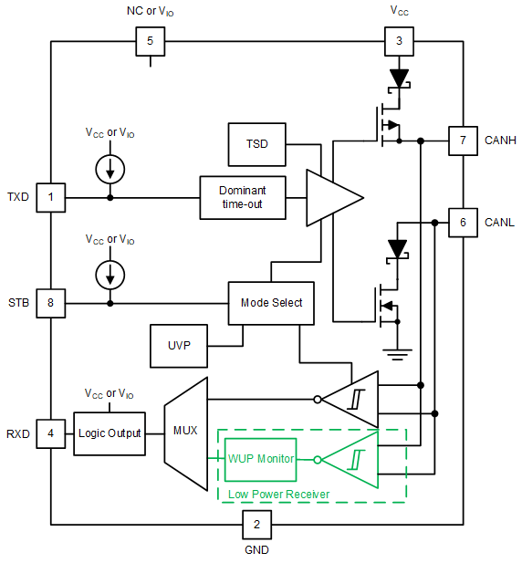
Figure 1-1 shows the device functional block diagram for reference. TCAN844-Q1 has the VIO input at pin 5, while TCAN844V-Q1 has a no connect (NC) at pin 5.
 Figure 1-1 TCAN844-Q1 and
TCAN844V-Q1 Functional Block Diagram