SGEA001A December   2019  – April 2021 SN74LVC1G125-Q1


  1.   Trademarks
  2. 1Block Diagram
  3. 2Optimizing Gate Driver Control and MCU Communication
  4. 3Logic and Translation Use Cases
    1. 3.1 Logic Use Cases
      1. 3.1.1 Increase Drive Strength
      2. 3.1.2 Gate Driver Control
      3. 3.1.3 Low-Power CAN Wake
    2. 3.2 Voltage Translation Use Cases
      1. 3.2.1 Non-Isolated SPI Communication
      2. 3.2.2 Non-Isolated UART Communication
  5. 4Recommended Logic and Translation Families for On-Board and Wireless Chargers
    1. 4.1 LVC: Low-Voltage CMOS Logic and Translation
    2. 4.2 HCS: Schmitt-Trigger Integrated High-Speed CMOS Logic
  6. 5Revision History

Block Diagram

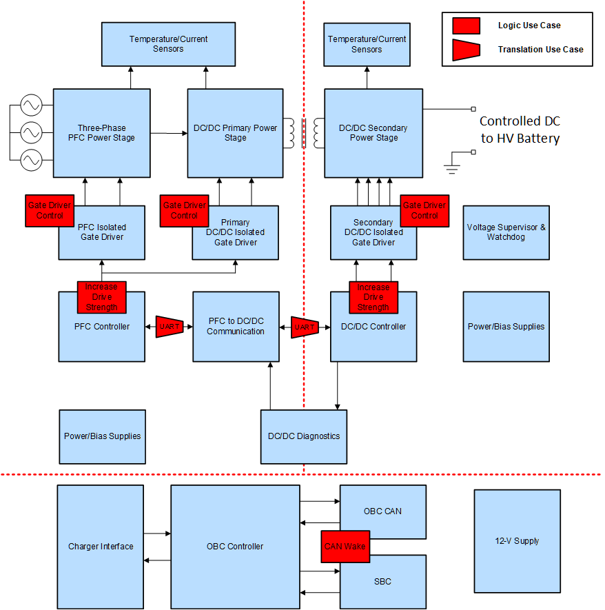
GUID-A5525A0A-9F75-46ED-B66B-464716EE8F78-low.gifFigure 1-1 Simplified Block Diagram for On-Board and Wireless Charger Systems

See On-Board and Wireless Chargers for a more complete view of the interactive online End Equipment Reference Diagram.