SGLS148F December 2002 – June 2024 ULQ2003A-Q1 , ULQ2004A-Q1
PRODUCTION DATA
- 1
- 1 Features
- 2 Applications
- 3 Description
- 4 Pin Configuration and Functions
-
5 Specifications
- 5.1 Absolute Maximum Ratings
- 5.2 ESD Ratings
- 5.3 Recommended Operating Conditions
- 5.4 Thermal Information
- 5.5 Electrical Characteristics, ULQ2003AT and ULQ2003AQ
- 5.6 Electrical Characteristics, ULQ2004AT
- 5.7 Switching Characteristics, ULQ2003A and ULQ2004A
- 5.8 Dissipation Ratings
- 5.9 Typical Characteristics
- 6 Parameter Measurement Information
- 7 Detailed Description
- 8 Application and Implementation
- 9 Device and Documentation Support
- 10Revision History
- 11Mechanical, Packaging, and Orderable Information
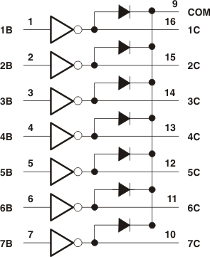
7.2 Functional Block Diagram
 Figure 7-1 Logic Diagram
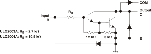
A. All resistor values shown are nominal.
B. The collector-emitter diode is a parasitic structure and should not be used to conduct current. If the collector(s) go below ground an external Schottky diode should be added to clamp negative undershoots.
Figure 7-2 Schematics (Each Darlington Pair)