SGLS246B June 2004 – October 2016 TPS60400-Q1 , TPS60401-Q1 , TPS60402-Q1 , TPS60403-Q1
PRODUCTION DATA.
- 1 Features
- 2 Applications
- 3 Description
- 4 Revision History
- 5 Device Comparison Table
- 6 Pin Configuration and Functions
- 7 Specifications
- 8 Detailed Description
- 9 Application and Implementation
- 10Power Supply Recommendations
- 11Layout
- 12Device and Documentation Support
- 13Mechanical, Packaging, and Orderable Information
8 Detailed Description
8.1 Overview
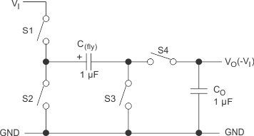
The TPS6040x-Q1 charge pumps invert the voltage applied to their input. For the highest performance, use low equivalent series resistance (ESR) capacitors (for example, ceramic). During the first half-cycle, switches S2 and S4 open, switches S1 and S3 close, and capacitor (C(fly)) charges to the voltage at VI. During the second half-cycle, S1 and S3 open, and S2 and S4 close. This connects the positive terminal of C(fly) to GND and the negative to VO. By connecting C(fly) in parallel, CO is charged negative. The actual voltage at the output is more positive than −VI, since switches S1–S4 have resistance and the load drains charge from CO.
 Figure 20. Operating Principle
8.2 Functional Block Diagram

8.3 Feature Description
8.3.1 Charge-Pump Output Resistance
The TPS6040x-Q1 devices are not voltage regulators. The output source resistance of the charge pumps is approximately 15 Ω at room temperature (with VI = 5 V), and VO approaches –5 V when lightly loaded. VO will droop toward GND as load current increases as seen in Equation 1.

8.3.2 Efficiency Considerations
The power efficiency of a switched-capacitor voltage converter is affected by three factors: the internal losses in the converter IC, the resistive losses of the capacitors, and the conversion losses during charge transfer between the capacitors. The internal losses are associated with the internal functions of the ICs, such as driving the switches, oscillator, and so forth. These losses are affected by operating conditions such as input voltage, temperature, and frequency. The next two losses are associated with the voltage converter circuit’s output resistance. Switch losses occur because of the on-resistance of the MOSFET switches in the IC. Charge-pump capacitor losses occur because of their ESR. The relationship between these losses and the output resistance is Equation 3.

The first term is the effective resistance from an ideal switched-capacitor circuit. Conversion losses occur during the charge transfer between C(fly) and CO when there is a voltage difference between them. The power loss is Equation 4.

The efficiency of the TPS6040x-Q1 devices is dominated by their quiescent supply current at low output current and by their output impedance at higher current (see Equation 5).

where
- IQ = quiescent current
8.4 Device Functional Modes
8.4.1 Active-Schottky Diode
For a short period of time, when the input voltage is applied, but the inverter is not yet working, the output capacitor is charged positive by the load. To prevent the output being pulled above GND, a Schottky diode must be added in parallel to the output. The function of this diode is integrated into the TPS6040x-Q1 devices, which gives a defined startup performance and saves board space.
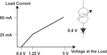
A current sink and a diode in series can approximate the behavior of a typical, modern operational amplifier. Figure 21 shows the current into this typical load at a given voltage. The TPS6040x-Q1 devices are optimized to start into these loads.
 Figure 21. Typical Load
 Figure 22. Maximum Start-Up Current
