SGLS380I September   2008  – May 2024 TL720M05-Q1

PRODMIX  

  1.   1
  2. Features
  3. Applications
  4. Description
  5. Pin Configuration and Functions
  6. Specifications
    1. 5.1 Absolute Maximum Ratings
    2. 5.2 ESD Ratings
    3. 5.3 Recommended Operating Conditions
    4. 5.4 Thermal Information
    5. 5.5 Electrical Characteristics
    6. 5.6 Typical Characteristics
  7. Parameter Measurement Information
  8. Detailed Description
    1. 7.1 Overview
    2. 7.2 Functional Block Diagrams
    3. 7.3 Feature Description
      1. 7.3.1 Undervoltage Lockout
      2. 7.3.2 Thermal Shutdown
      3. 7.3.3 Current Limit
    4. 7.4 Device Functional Modes
      1. 7.4.1 Normal Operation
      2. 7.4.2 Dropout Operation
      3. 7.4.3 Disabled
  9. Application and Implementation
    1. 8.1 Application Information
      1. 8.1.1 Input and Output Capacitor Selection
        1. 8.1.1.1 Legacy Chip Capacitor Selection
        2. 8.1.1.2 New Chip Output Capacitor
        3. 8.1.1.3 New Chip Input Capacitor
      2. 8.1.2 Dropout Voltage
      3. 8.1.3 Reverse Current
      4. 8.1.4 Power Dissipation (PD)
        1. 8.1.4.1 Thermal Performance Versus Copper Area
        2. 8.1.4.2 Power Dissipation Versus Ambient Temperature
      5. 8.1.5 Estimating Junction Temperature
    2. 8.2 Typical Application
      1. 8.2.1 Design Requirements
      2. 8.2.2 Detailed Design Procedure
        1. 8.2.2.1 Input Capacitor
        2. 8.2.2.2 Output Capacitor
      3. 8.2.3 Application Curves
    3. 8.3 Power Supply Recommendations
    4. 8.4 Layout
      1. 8.4.1 Layout Guidelines
      2. 8.4.2 Layout Examples
  10. Device and Documentation Support
    1. 9.1 Device Support
      1. 9.1.1 Evaluation Module
      2. 9.1.2 Device Nomenclature
      3. 9.1.3 Development Support
    2. 9.2 Documentation Support
      1. 9.2.1 Related Documentation
    3. 9.3 Receiving Notification of Documentation Updates
    4. 9.4 Support Resources
    5. 9.5 Trademarks
    6. 9.6 Electrostatic Discharge Caution
    7. 9.7 Glossary
  11. 10Revision History
  12. 11Mechanical, Packaging, and Orderable Information

Current Limit

The device has an internal current limit circuit that protects the regulator during transient high-load current faults or shorting events. The current limit is a brick-wall scheme. In a high-load current fault, the brick-wall scheme limits the output current to the current limit (ICL). ICL is listed in the Electrical Characteristics table.

The output voltage is not regulated when the device is in current limit. When a current limit event occurs, the device begins to heat up because of the increase in power dissipation. When the device is in brick-wall current limit, the pass transistor dissipates power [(VIN – VOUT) × ICL]. If thermal shutdown is triggered, the device turns off. After the device cools down, the internal thermal shutdown circuit turns the device back on. If the output current fault condition continues, the device cycles between current limit and thermal shutdown. For more information on current limits, see the Know Your Limits application note.

Figure 7-3 shows a diagram of the current limit.
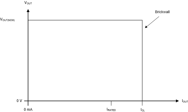
TL720M05-Q1 Current
          Limit Figure 7-3 Current Limit