SGLS380I September 2008 – May 2024 TL720M05-Q1
PRODMIX
- 1
- 1 Features
- 2 Applications
- 3 Description
- 4 Pin Configuration and Functions
- 5 Specifications
- 6 Parameter Measurement Information
- 7 Detailed Description
- 8 Application and Implementation
- 9 Device and Documentation Support
- 10Revision History
- 11Mechanical, Packaging, and Orderable Information
5.6 Typical Characteristics
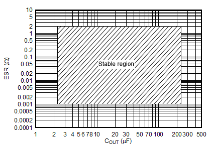
specified for new chip at TJ = –40°C to +150°C, VIN = 13.5V , IOUT = 100μA, COUT = 2.2µF, 1mΩ < COUT ESR < 2Ω, and CIN = 1µF (unless otherwise noted)

(Legacy Chip)
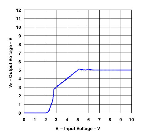
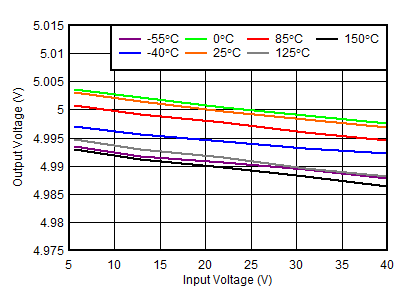
| VOUT = 5V, IOUT = 150mA |
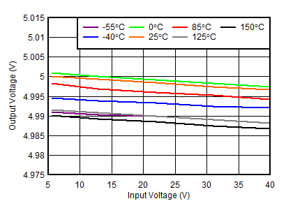
| VOUT = 5V, IOUT = 1mA |
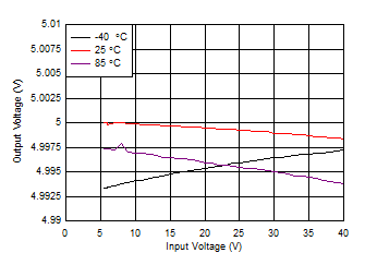
| COUT = 10µF, VOUT = 5V |
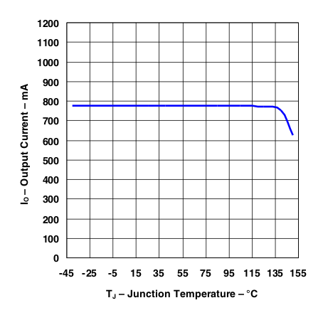
(Legacy Chip)
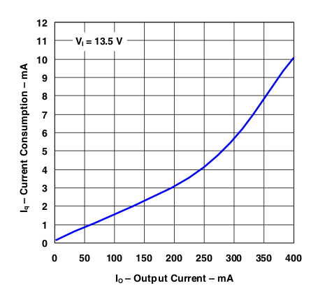
(Legacy Chip)
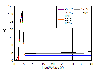
| VOUT = 5V |
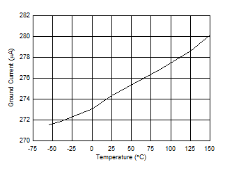
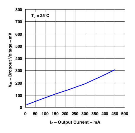
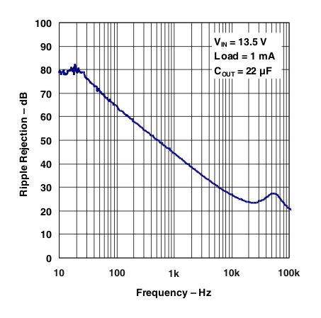
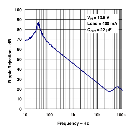
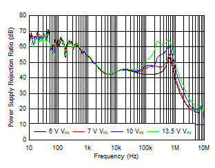
| COUT = 10µF (X7R 50V), IOUT = 500mA, VOUT = 5V |
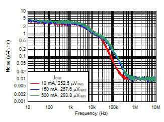
| COUT = 10µF (X7R 50V), VOUT = 3.3V | ||
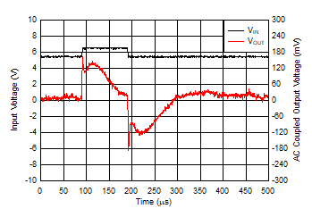
| VOUT = 5V, IOUT = 100mA,
VIN = 5.5V to 6.5V, rise time = 1µs |
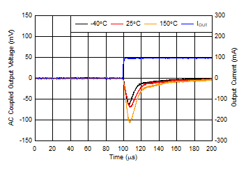
| VOUT = 5V, IOUT = 0mA to
100mA, slew rate = 1A/µs, COUT = 10µF |
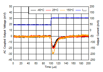
| VOUT = 5V, IOUT = 45mA to
105mA, slew rate = 0.1A/µs, COUT = 10µF |
(New Chip)
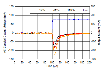
| VOUT = 5V, IOUT = 0mA to
150mA, slew rate = 1A/µs, COUT = 10µF |
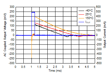
| VOUT = 5V, IOUT = 0mA to
500mA, slew rate = 1A/µs, COUT = 10µF |
(New Chip)
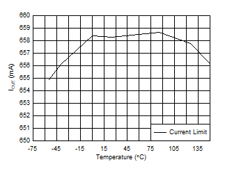
| VIN = VOUT + 1V, VOUT = 90% × VOUT(NOM) |
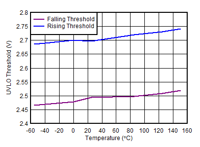
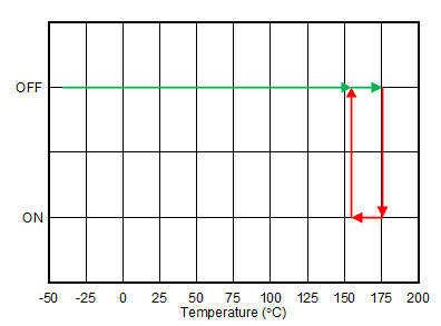
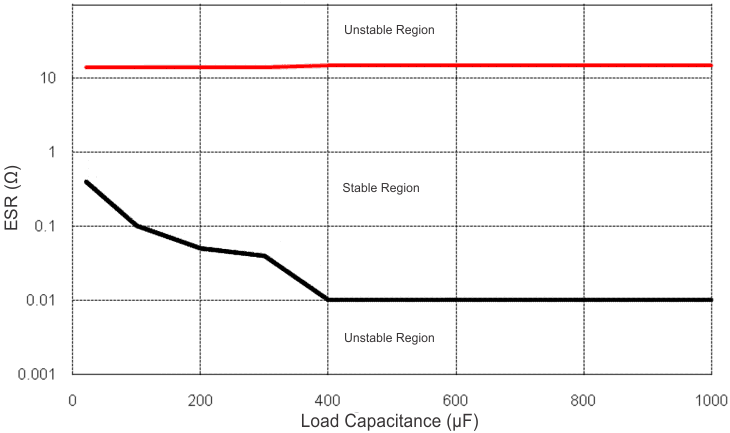
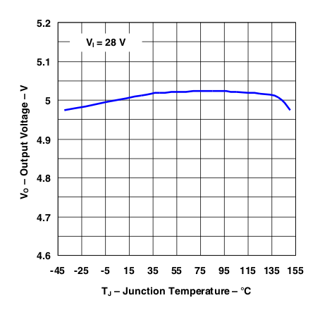
(Legacy Chip)
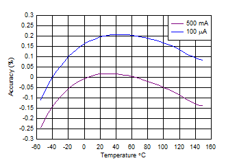
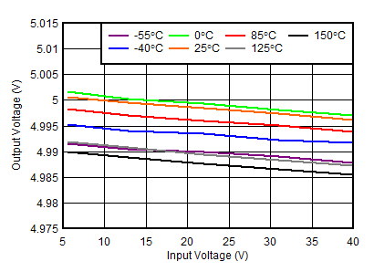
| VOUT = 5V, IOUT = 5mA |
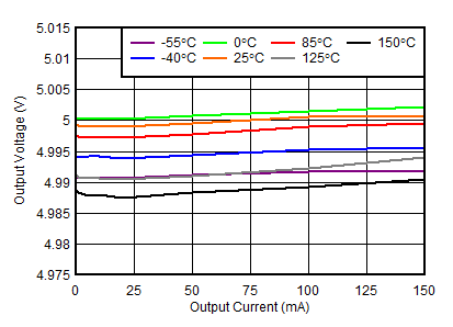
| VOUT = 5V |
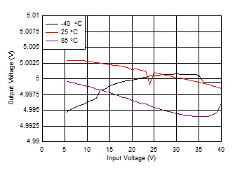
| COUT = 10µF, VOUT = 5V |
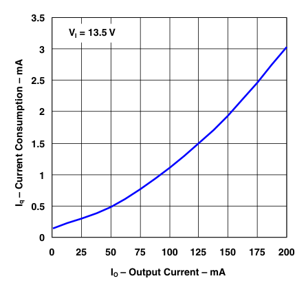
(Legacy Chip)
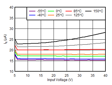
(New Chip)
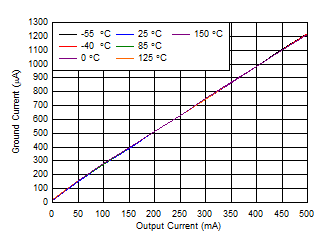
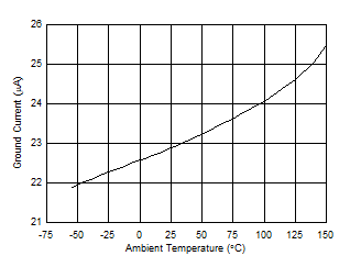
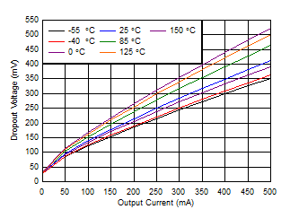
| VIN = 3V |
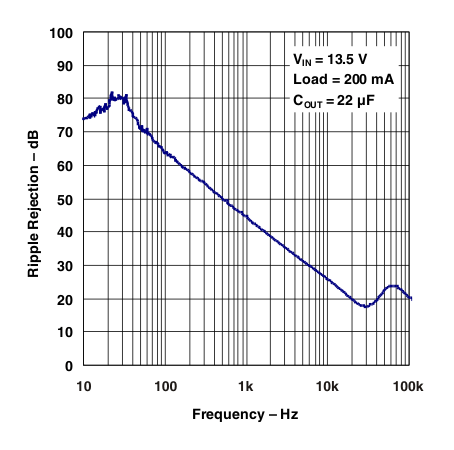
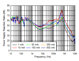
| COUT = 10µF (X7R 50V), VOUT = 5V |
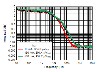
| COUT = 10µF (X7R 50V), VOUT = 5V |
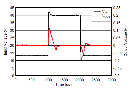
| VOUT = 5V, IOUT = 1mA,
VIN = 13.5V to 45V, slew rate = 2.7V/µs |
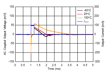
| VOUT = 5V, IOUT = 0mA to
100mA, slew rate = 1A/µs, COUT = 10µF |
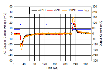
| VOUT = 5V, IOUT = 45mA to
105mA, slew rate = 0.1A/µs, COUT = 10µF |
(New Chip)
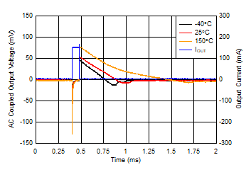
| VOUT = 5V, IOUT = 0mA to
150mA, slew rate = 1A/µs, COUT = 10µF |
(New Chip)
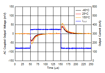
| VOUT = 5V, IOUT = 150mA to 350mA, slew rate = 0.1A/µs, COUT = 10µF |
(New Chip)
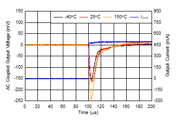
| VOUT = 5V, IOUT = 0mA to
500mA, slew rate = 1A/µs, COUT = 10µF |
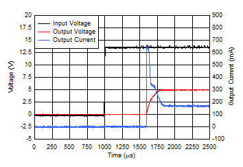
| VIN = VOUT + 1V, VOUT = 90% × VOUT(NOM) |
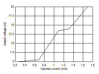
(New Chip)

