SLAA202B February 2005 – December 2018 MSP430F149 , MSP430F149 , MSP430F2252-Q1 , MSP430F2252-Q1 , MSP430F2272-Q1 , MSP430F2272-Q1 , MSP430F2274 , MSP430F2274 , MSP430FG4619 , MSP430FG4619
-
Implementing IrDA With MSP430™ MCUs
- Trademarks
- 1 Introduction
- 2 Hardware Description
- 3 Software Description
- 4 PC Demonstration Application
- 5 IrDA Protocol Basics
- 6 IrDA Communication Diagram
- 7 Frame Exchange Log
- 8 References
- Revision History
2.2 Circuit Description
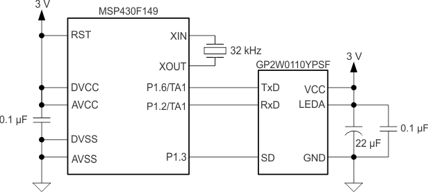
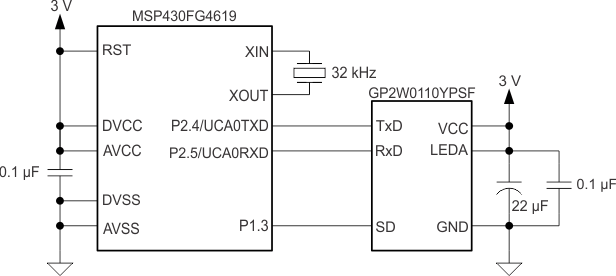
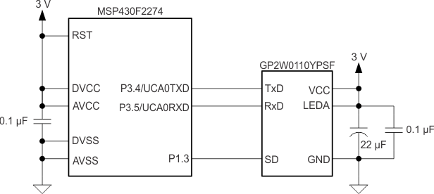
The circuitry around the GP2W0110YPSF is simple (see Figure 1). Two pins are connected to the 3.0-V supply voltage (VCC and LEDA), one pin is connected to the common ground, and three pins interface to the MSP430 (TxD, RxD, and SD). Two bypass capacitors are placed in parallel between VCC and ground close to the transceiver to compensate for current pulses that occur when the transmit IR LED is operated. The TxD and RxD connections are made to Timer_A pins in case of the MSP430F149 (see Figure 1), and to USCI_A0 pins in case of the MSP430FG4619 (see Figure 2) and the MSP430F2274 (see Figure 3).
For the MSP430F149-based design, the device is sourced by a 32-kHz watch crystal that provides a reference clock to calibrate the internal high-speed DCO using a software FLL. This configuration is needed to meet the requirements of the IrPHY physical layer timing specification.
The MSP430FG4619-based design also uses a 32-kHz watch crystal. However, in this case, the built-in FLL circuit of the device clock module generates the system clock.
No external crystal is needed for the MSP430F2274-based design. In this case, the factory-provided DCO calibration constants are loaded into the DCO during device startup, to provide an accurate and stable system clock.
 Figure 1. Schematic Using MSP430F149
  Figure 2. Schematic Using MSP430FG4619
  Figure 3. Schematic Using MSP430F2274