SLAA202B February 2005 – December 2018 MSP430F149 , MSP430F149 , MSP430F2252-Q1 , MSP430F2252-Q1 , MSP430F2272-Q1 , MSP430F2272-Q1 , MSP430F2274 , MSP430F2274 , MSP430FG4619 , MSP430FG4619
-
Implementing IrDA With MSP430™ MCUs
- Trademarks
- 1 Introduction
- 2 Hardware Description
- 3 Software Description
- 4 PC Demonstration Application
- 5 IrDA Protocol Basics
- 6 IrDA Communication Diagram
- 7 Frame Exchange Log
- 8 References
- Revision History
3.1.2 Reception
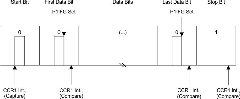
Reception is based not on trying to capture the pulse when it comes in but is instead based on latching the input and testing for the presence of a pulse some time after the bit has been sent by the primary. Therefore, the interrupt flag for the port pin is checked before the time allocated for sending the bit is over. The main reason for this implementation is that 3/16th of a pulse does not allow much room for error and if reception is off by a small percentage, then more bits could be missed and the frame would be corrupted.
The pointer to the buffer is incremented, and the following bytes are stored through the same process until the EOF flag is encountered. Finally, the pointer is offset to the next location in memory. When idle, the application is always in receive mode waiting for an incoming start bit.
The process through which each byte is received depends on the IrDA_RX routine and the TA1_ISR. To receive:
- A bit counter is loaded with 8 bits, the clock source for Timer_A is set to SMCLK, and the mode control bits are set to use the timer in continuous mode.
- The capture/compare block 1 is configured to capture the falling edge of the input signal synchronized with the timer clock (SMCLK), and interrupts are also enabled.
- When the ISR is done collecting the bits, it clears the CCIE flag, indicating that the reception of one byte has finished.
Every time the TA1_ISR is called, it adds the time to the next bit to CCR1 and tests CCTL1 for its capture/compare setting. If it is in capture mode, then the start bit is being handled. The routine adds an additional quarter of the bit length to the value in CCR1 which now holds a total of one and a quarter bit length and then sets the pin to I/O function. The I/O interrupt edge select is set to be triggered on a high-to-low transition (register P1IES), and the interrupt flag is cleared (register P1IFG) to clear the latched edge. After this, a switch is made to compare mode before returning from the ISR.
If the test for the capture/compare setting of CCTL1 results in a 0, there are incoming data bits. The P1IFG flag for the I/O pin is then tested. If the bit is set, a 0 was received, and if the bit is not set, a 1 was received. Next, the received bit is rotated through the use of an RRC instruction into the IR_DATA variable which holds the byte being received.
The received bit is then inverted, and the edge latch is cleared. Finally, the counter for bit reception is decremented by 1. If the counter is not 0, then the interrupts continue to be enabled and because, at the return from the interrupt, the CCIE flag is still not 0, the next incoming data bits are processed until the counter reaches 0 and interrupts are stopped. At this point, the entire byte has been successfully received. Figure 6 shows this process.
 Figure 6. Detailed Byte Reception