SLAA202B February 2005 – December 2018 MSP430F149 , MSP430F149 , MSP430F2252-Q1 , MSP430F2252-Q1 , MSP430F2272-Q1 , MSP430F2272-Q1 , MSP430F2274 , MSP430F2274 , MSP430FG4619 , MSP430FG4619
-
Implementing IrDA With MSP430™ MCUs
- Trademarks
- 1 Introduction
- 2 Hardware Description
- 3 Software Description
- 4 PC Demonstration Application
- 5 IrDA Protocol Basics
- 6 IrDA Communication Diagram
- 7 Frame Exchange Log
- 8 References
- Revision History
3.1.1 Transmission
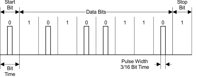
For transmission, the initial XBOF flags are sent first followed by the BOF flag. Then the rest of the frame is transmitted. The FCS is calculated and sent after the whole frame has been sent, followed by the EOF flag. The actual sending of the individual bytes is performed by fitting each bit into 3/16th of a pulse, where a 0 is represented by a pulse and a 1 is represented by no pulse (see Figure 4). The transmission process is interrupt driven and is handled by the Timer_A module.
 Figure 4. IR Byte
 The actual encoding is manipulated in its entirety by the Timer_A module.
- The bit length and 3/16th of the bit length are calculated given the speed at which the Timer_A clock source is operating, and they are stored as constants for use in the transmission process.
- Timer_A is cleared and the clock source is set to SMCLK.
- The pin being used for transmitting data is configured for the CCR1 peripheral function, and its direction is set to output.
- The current state of TAR is stored in register CCR1 which, given that TAR has been previously cleared, holds a value of 0.
- One bit length is added to the value stored in CCR1, and then CCR1 is copied into register CCR0.
- The number of counts that equal 3/16th of a pulse width is added to CCR0.
- The stop bit and start bit are added to the 8 bits of data to be transmitted.
- The transmission counter is loaded with 10, to include the start and stop bits.
- The CCR0 interrupt is enabled in the CCTL0 control register.
- Output Mode 3 Set/Reset is selected for CCR1 to transmit the start bit.
- Timer_A is started in continuous mode.
- The CCIE flag is polled to determine when the transmission has ended, because the ISR clears the CCIE flag when all bits of the byte have been transmitted. The CCIE flag is polled by a subroutine inside the transmission routine and as soon as the CCIE flag is cleared, the transmission routine returns.
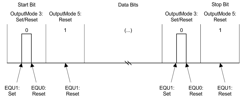
- When TAR reaches CCR1, the output goes high and it returns back low when TAR reaches CCR0. This generates the start bit.
Figure 5 shows the switching between the output modes as well as the resulting output signals.
- The Timer_A module first adds 1 bit length to CCR1 and CCR0. This keeps them 3/16th of a bit apart from each other but sets them up in time to transmit the next bit.
- If the bit is 0, then it is sent using Output Mode 3 Set/Reset which produces a pulse, given that all bits must be sent inverted.
- If the bit is 1, then Output Mode 3 is changed to Output Mode 5 Reset to make sure that the output is held low.
- When the bit counter reaches 0, the interrupts for CCR0 are disabled and the ISR returns.
 Figure 5. Transmission With Timer_A