SLAA867A December 2018 – September 2024 DAC80501 , DAC80508 , DAC8775
Design Goals
| Supply Voltage (VCC) | DAC Output Voltage | Output Current | Error | Max Load Resistance | Compliance Voltage |
|---|---|---|---|---|---|
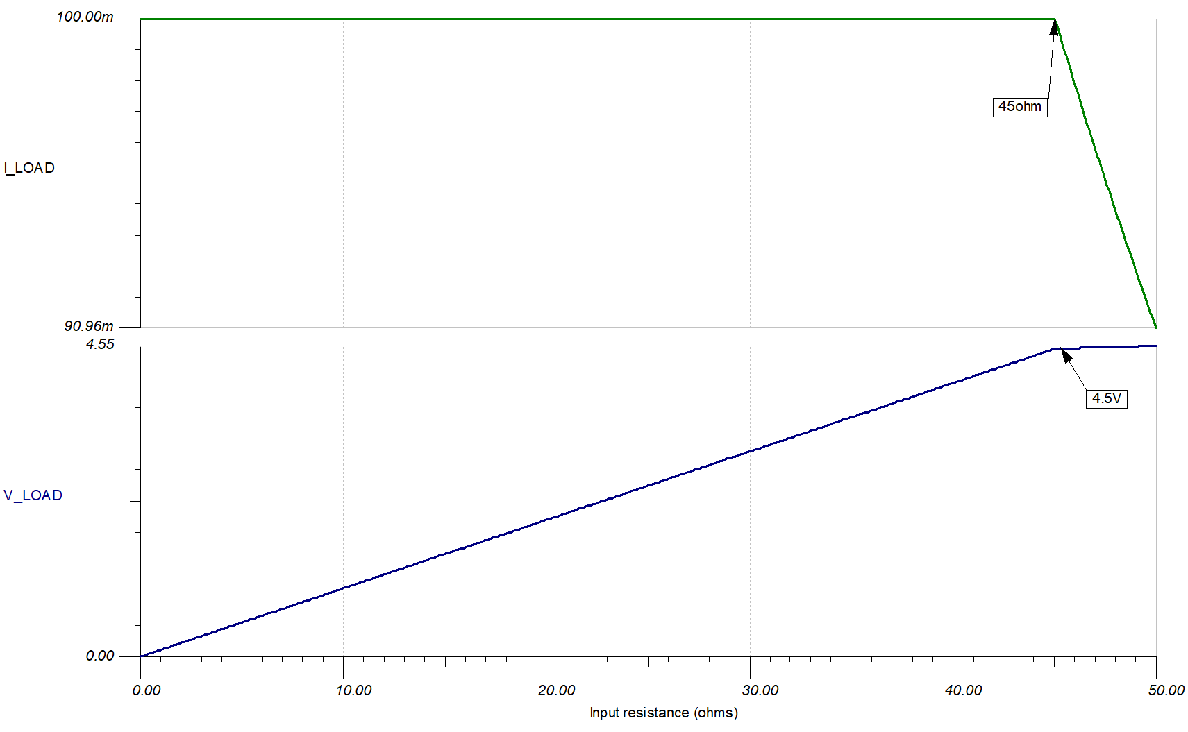
| 5V | 0V–2V | 0–100mA | <1% FSR | 45Ω | 4.5V |
Design Description
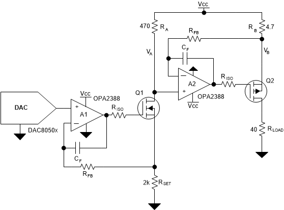
The programmable high-side current source supplies an adjustable current to a ground reference load. The first op amp stage sets a reference current based on the DAC output voltage. The second op amp stage acts as a current mirror that gains the reference current and regulates the current sourced from the output PMOS to the load. RSET, RA, and RB set the output current based on the DAC voltage. Components CCOMP, RISO, and RFB provide compensation to verify the stability of the circuit. Common end equipment that utilize this circuit include PLC Analog Output Modules, Field Transmitters, Digital Multimeters, Printers, Optical Modules, LED Drivers, and EPOS.

Design Notes
- Choose a DAC with low offset, gain, and drift errors. Use RRIO op amps to maintain low compliance voltage and op amps with low offset should be selected.
- Minimize the current flow through RA, Q1, and RSETby selecting a large ratio of RA:RB to maximize efficiency while also minimizing heating and drift in the first stage.
- Use high-precision, low-drift resistors for RSET, RA, and RB to minimize error caused by resistor mismatch and temperature drift.
- Minimize the resistance of RB to maximize compliance voltage.
- Avoid placing Q2 near thermally sensitive components in layout as the power dissipation causes heating.
Design Steps
- Set the reference current in the sink stage by selecting
RSET based on VDAC. Minimize the reference current as
it flows directly to ground and reduced efficiency. Set the reference current to
1mA and calculate RSET.

- Select the required gain ratio based on the desired output current and IOUT/ISET = 100mA/1mA = 100, this is the required ratio of RA:RB.
- Calculate the maximum value of RB from the maximum
allowable voltage drop to drive the maximum current through the maximum load.

- The voltage VA is VCC –
ISETxRA which is equal to the voltage VB
due to the op amp feedback. Select RA to achieve a voltage drop of
<500mV to maintain the desired compliance voltage. A standard resistance of
4.7Ω is chosen.


- Calculate RB based on RA and the gain
selected in step 2.

- Verify the power dissipation of Q2. The power dissipation of Q2
based on the load is given by:

The maximum power dissipation of Q2 occurs when the load resistance is zero:

Confirm that Q2 is rated for this power dissipation.
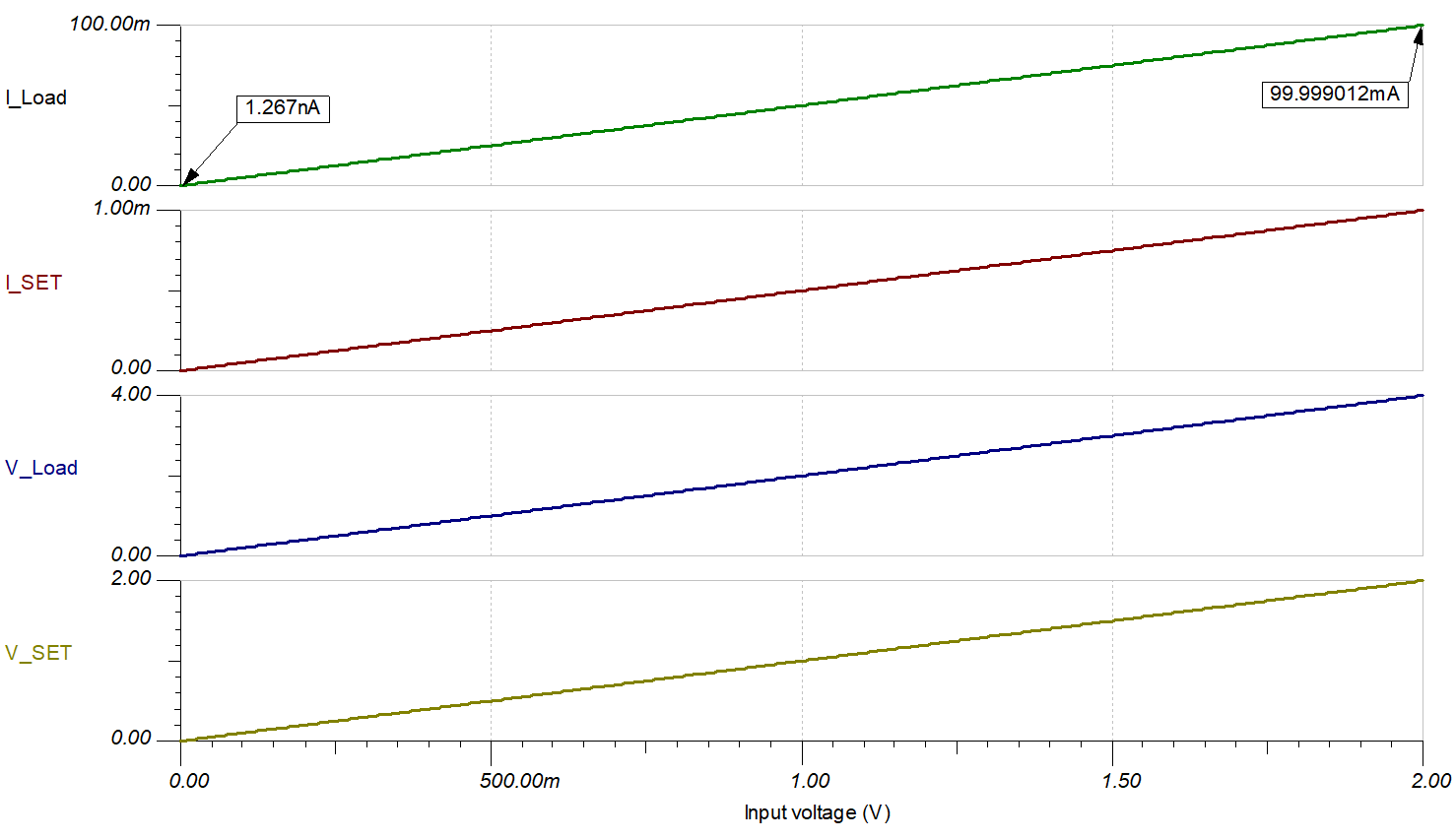
DC Transfer Characteristics

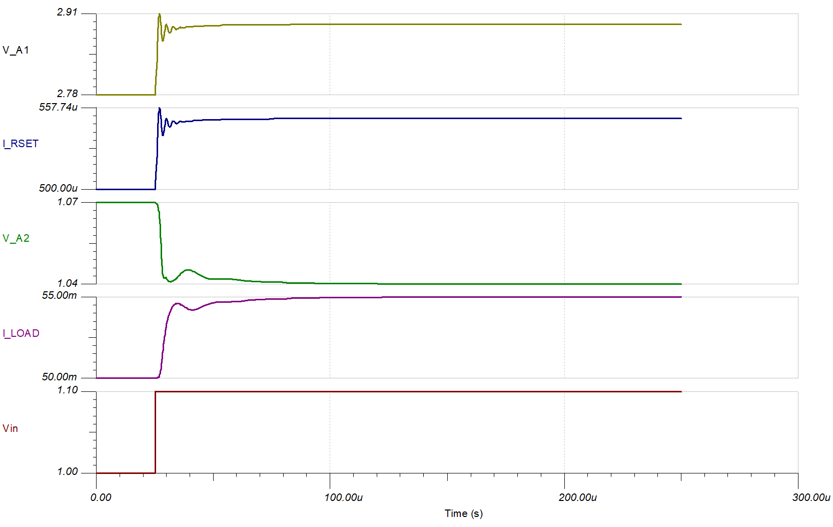
Small-Signal Step Response

Compliance Voltage

High Voltage Supply Modification
This circuit design example uses a low voltage supply for VCC. Some applications, such as 4mA – 20mA current loops, require a high voltage supply to drive large resistive loads. To modify this current source for higher voltage supply, choose a high voltage, rail-to-rail input/output amplifier such as OPA192.
Devices
Links to Key Files
Texas Instruments, High side V-I converter reference design from 0V to 2V and 0mA to 100mA, 1% full-scale error, TIPD102 overview
Texas Instruments, Less Than 1-W, Quad-Channel, Analog Output Module With Adaptive Power Management Reference Design, TIPD215 overview
Texas Instruments, 8-channel, 16-bit, 200mA current output DAC, reference design
Texas Instruments, source files for SLAA867, software support