SLAA926B December 2019 – October 2024 MSP430FR2310 , MSP430FR2311 , MSP430FR2353 , MSP430FR2355
Design Goals
| Input | Output | BW | Supply | |||
|---|---|---|---|---|---|---|
| IiMin | IiMax | VoMin | VoMax | fp | Vcc | Vee |
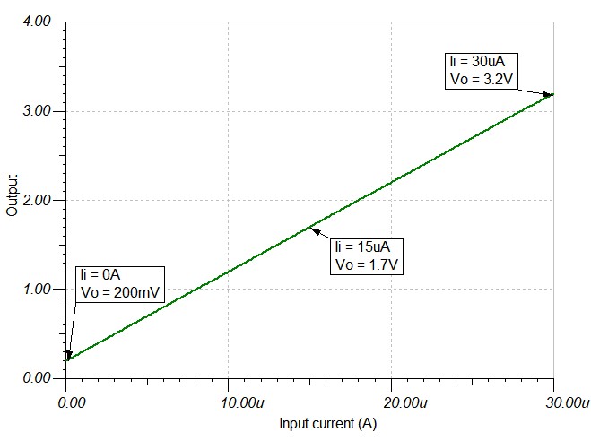
| 0 A | 30 µA | 0.2V | 3.2V | 10 kHz | 3.3V | 0V |
Design Description
Some MSP430™ microcontrollers (MCUs) contain configurable integrated signal chain elements such as op-amps, DACs, and programmable gain stages. These elements make up a peripheral called the smart analog combo (SAC). For information on the different types of SACs and how to leverage their configurable analog signal chain capabilities, see the MSP430 MCUs Smart Analog Combo video. To get started with your design, download the MSP430 Transimpedance Amplifier Circuit Design Files.
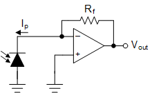
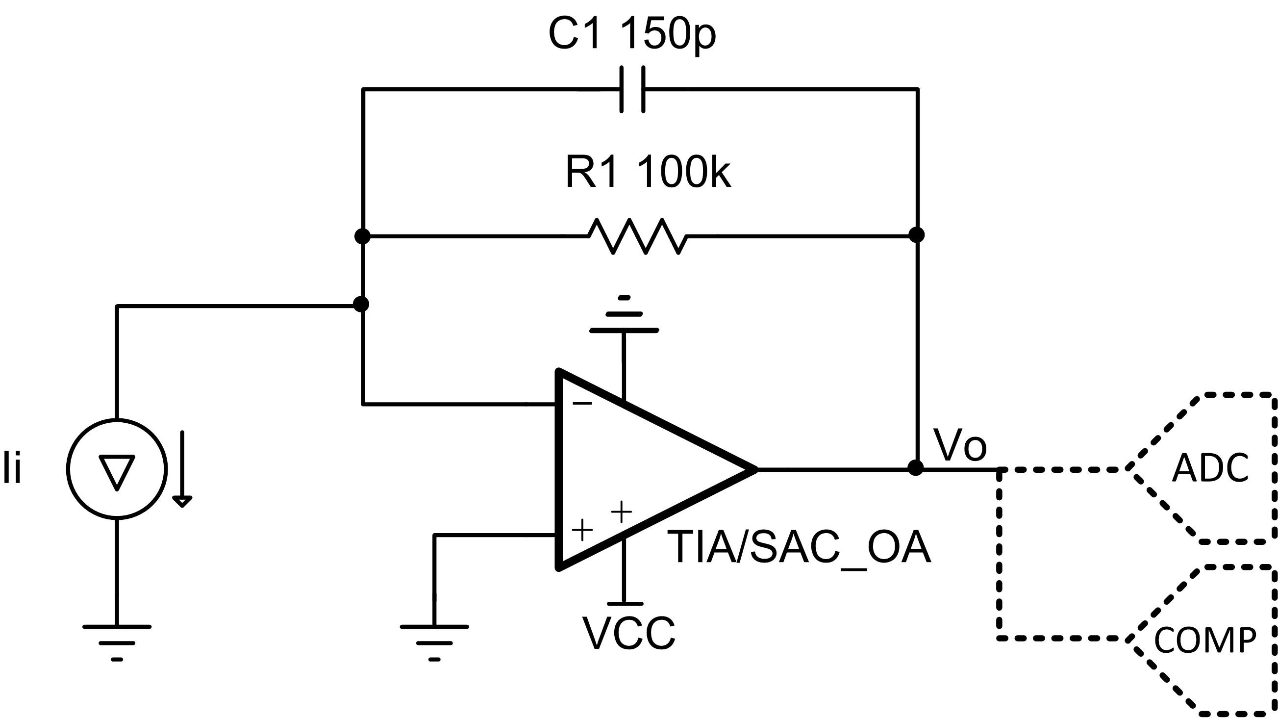
The transimpedance op amp circuit configuration converts an input current source into an output voltage. The current to voltage gain is based on the feedback resistance. The circuit can maintain a constant voltage bias across the input source as the input current changes, which benefits many sensors. The characteristics of the Transimpedance Amplifier (TIA) module in MSP430FR2311 make it especially suited for this functionality; however, this circuit can also be implemented with the MSP430FR2311, or with the MSP430FR2355 with additional built-in DAC and PGA capabilities. The output of these integrated amplifiers can be sampled directly by the on-board ADC or monitored by the on-board comparator for further processing inside the MCU.
Design Notes
- An op amp with low input bias current reduces DC errors.
- A bias voltage can be added to the non-inverting input to set the output voltage for 0-A input currents. The integrated 12-bit DAC in MSP430FR2355 SAC_L3 can be used for this purpose.
- Operate within the linear output voltage swing (see Aol specification) to minimize non-linearity errors.
- If the fix is implemented with the MSP430FR2311, this circuit can be realized by the TransImpedance Amplifier (TIA) module, or by the SAC_L1.
- If the fix is implemented with the MSP430FR2355 SAC_L3, the op-amp should be configured in general-purpose mode.
- The MSP430 Transimpedance Amplifier Circuit Design Files include code examples showing how to properly initialize the peripherals.
Design Steps
- Select the gain resistor.
- Select the feedback capacitor to
meet the circuit bandwidth.
- Calculate the necessary op amp gain
bandwidth (GBW) for the circuit to be stable.
Design Simulations
DC Simulation Results
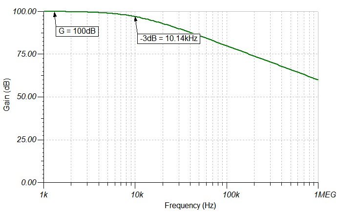
AC Simulation Results
Target Applications
Design References
- Texas Instruments, MSP430 Transimpedance Amplifier, code examples and SPICE simulation files
- Texas Instruments, MSP430FR2311 16MHz integrated analog microcontroller with 3.75KB FRAM, Op Amp, TIA, comparator with DAC, 10-bit ADC, product page
- Texas Instruments, MSP430 MCUs Smart Analog Combo, video
Design Featured Op Amp
| MSP430FR2311 Transimpedance Amplifier | |
|---|---|
| Vcc | 2.0V to 3.6V |
| VCM | -0.1V to VCC/2V |
| Vout | Rail-to-rail |
| Vos | ±5mV |
| AOL | 100dB |
| Iq | 350µA (high-speed mode) |
| 120µA (low-power mode) | |
| Ib | 5pA (TSSOP-16 with OA-dedicated pin input) |
| 50pA (TSSOP-20 and VQFN-16) | |
| UGBW | 5MHz (high-speed mode) |
| 1.8MHz (low-power mode) | |
| SR | 4V/µs (high-speed mode) |
| 1V/µs (low-power mode) | |
| Number of channels | 1 |
| MSP430FR2311 | |
Design Alternate Op Amp
| MSP430FRxx Smart Analog Combo | ||
|---|---|---|
| MSP430FR2311 SAC_L1 | MSP430FR2355 SAC_L3 | |
| Vcc | 2.0V to 3.6V | |
| VCM | -0.1V to VCC + 0.1V | |
| Vout | Rail-to-rail | |
| Vos | ±5mV | |
| AOL | 100dB | |
| Iq | 350µA (high-speed mode) | |
| 120µA (low-power mode) | ||
| Ib | 50pA | |
| UGBW | 4MHz (high-speed mode) | 2.8MHz (high-speed mode) |
| 1.4MHz (low-power mode) | 1MHz (low-power mode) | |
| SR | 3V/µs (high-speed mode) | |
| 1V/µs (low-power mode) | ||
| Number of channels | 1 | 4 |
| MSP430FR2311 | MSP430FR2355 | |


