SLAA934A December 2019 – December 2024 TPS732-Q1
4.1 SOT-223 (DCQ) Package
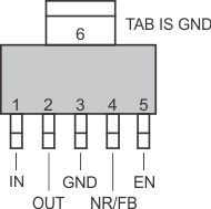
Figure 4-1 shows the TPS732-Q1 pin diagram for the SOT-223 (DCQ) package. For a detailed description of the device pins, see the Pin Configuration and Functions section in the TPS732-Q1 data sheet.
 Figure 4-1 Pin Diagram (SOT-223 (DCQ)) Package
Table 4-2 Pin FMA for Device Pins
Short-Circuited to Ground
| Pin Name | Pin No. | Description of Potential Failure Effects | Failure Effect Class |
|---|---|---|---|
| IN | 1 | Power is not supplied to the device. System performance depends on upstream current limiting. | B |
| OUT | 2 | Current limit is triggered, and the device can repeatedly enter and exit thermal shutdown depending on power dissipation. | B |
| GND | 3 | No effect. Normal operation. | D |
| NR/FB | 4 | [Fixed Output] The internal reference cannot start. The device cannot turn on. | B |
| EN | 5 | The device is disabled, resulting in no output voltage. | B |
Table 4-3 Pin FMA for Device Pins
Open-Circuited
| Pin Name | Pin No. | Description of Potential Failure Effects | Failure Effect Class |
|---|---|---|---|
| IN | 1 | No output voltage. | B |
| OUT | 2 | Output voltage is disconnected from load. | B |
| GND | 3 | Device biasing has no current path. The device is not operational and does not regulate. | B |
| NR/FB | 4 | [Fixed Output] Any noise-reduction benefits are lost. | C |
| EN | 5 | Device potentially disables. | B |
Table 4-4 Pin FMA for Device Pins
Short-Circuited to Adjacent Pin
| Pin Name | Pin No. | Shorted to | Pin No. | Description of Potential Failure Effects | Failure Effect Class |
|---|---|---|---|---|---|
| IN | 1 | OUT | 2 | Regulation is not possible. VOUT = VIN. If VIN exceeds 5.5V, damage is possible. | B |
| OUT | 2 | GND | 3 | Regulation is not possible. The device operates at current limit. The device can cycle in and out of thermal shutdown. | B |
| GND | 3 | NR/FB | 4 | Any noise-reduction benefits are lost. | C |
| NR/FB | 4 | EN | 5 | The output voltage is incorrect. | B |
Table 4-5 Pin FMA for Device Pins
Short-Circuited to
Supply
| Pin Name | Pin No. | Description of Potential Failure Effects | Failure Effect Class |
|---|---|---|---|
| IN | 1 | No effect. Normal operation. | D |
| OUT | 2 | Regulation is not possible. VOUT = VIN. If VIN exceeds 5.5V, damage is possible. | B |
| GND | 3 | No output voltage. System performance depends on the upstream current limit. | B |
| NR/FB | 4 | [Fixed Output] NR pin is damaged if VIN is higher than 6V. | A |
| EN | 5 | Device is always enabled. Regulation is possible. | B |