SLAA988A December 2020 – January 2022 TAS2563
1.11 Ground Planes
The ground plane routing is important when designing the PCB layout. These planes must be designed to have a proper thermal dissipation and minimize the parasitic impedance as much as possible. Design tips for the different ground pins are listed here:
- GND pin 28 must be treated like a signal, and connected to GND separately through a via. Do not pour GND plane over pins 27 and 28 together.
- All other ground pins must be shorted below the package and connected to the PCB ground plane through multiple vias.
- The vias are the best way to carry heat from the different sections in the board. Since the GND plane will need to quickly dissipate all the elevated temperatures, it is necessary to add multiple vias close to the ground pins.
- A maximum 150 pH of parasitic inductance is recommended. Having many vias reduces the additional impedance and provides good conduction in both electrical and thermal perspective.
- An entire layer immediately below the top layer must be dedicated to GND, as best practice.
 Figure 1-13 GND Pin 28
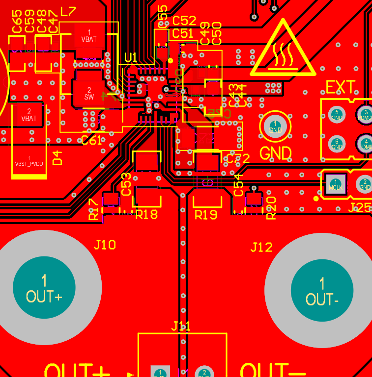
 Figure 1-14 TAS2x63 Top Layer
 Figure 1-15 TAS2x63 Layer 2
 Figure 1-16 TAS2x63 Layer 3
 Figure 1-17 TAS2x63 Bottom Layer