SLAA988A December 2020 – January 2022 TAS2563
3 Decoupling Capacitors
All the PCB routes have defined impedance that must be considered during all design stages. These signal paths will act as additional components in the board. In addition, the PCB lines have a parasitic inductance and capacitance that result in a different power distribution.
To reduce the negative effects of all these parasitic impedances, TI recommends that the VBAT and VDD decoupling capacitor connections respect the following rules:
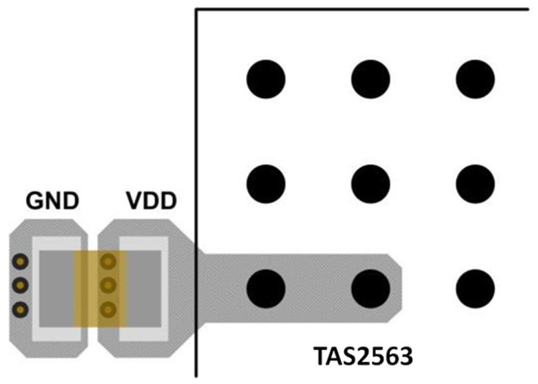
Place the decoupling capacitor close to the device pin in the same layer. The decoupling capacitor stores local charge and supplies the large transient currents when it is required. The TAS2563 device has many switching activity and voltage fluctuations that demand large current transients in a short period of time. In addition, the parasitic effects caused by the vias, traces, and pads generate a voltage drop in the power supply. The proximity of the decoupling capacitors to the power pins compensates these effects and supplies the large transient currents when it is required. On a multi-layer board, the capacitors must be placed in the same layer where the TAS2563 device is located. Otherwise, the decoupling capacitor value may be reduced by the additional capacitance due to the vias connections.
Place the VDD and GND vias as close as possible to the decoupling capacitors. If possible, place the vias directly or as close as possible to the capacitor mounting pads. The vias have defined impedance determined by its length and diameter. This impedance may cause a voltage drop (in highfrequency applications the signal integrity is greatly influenced) and a current flow that must be reduced or avoided. For that reason, TI recommends adding many vias around the mounting pads. This practice reduces the parasitic impedance.
 Figure 3-1 Decoupling Capacitor