SLAAE25 May 2021 MSP430FR2355 , MSP430FR2355
4 Hardware
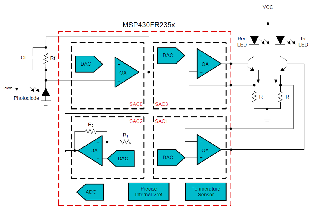
As shown in Figure 4-1, it shows the connection structure of the SAC inside FR235x.
- SAC0 as a TIA
- SAC2 as the gain stage
- ADC will capture SAC0 and SAC2 output
- SAC1 and SAC3 use to drive IR and RED LED.
From the structure in Figure 4-1, you can get the voltage of SAC0 output (Vo1):
Equation 3. 

The voltage of SAC2 output (Vo2):
Equation 4. 

In order to improve the SNR of the analog-to-digital converter (ADC) signal, the output signal of SAC2 needs to be adjusted at ADC VREF/2. Therefore, the value of DAC2 needs to be adjusted in real time according to the output of SAC0.
Equation 5. 

 Figure 4-1 Block Diagram of 4*SAC for Pulse
Oximeter
Figure 4-1 Block Diagram of 4*SAC for Pulse
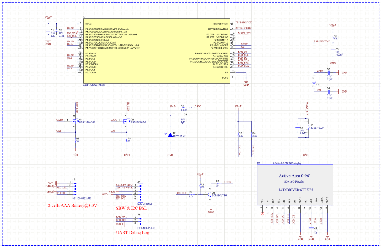
OximeterIn the schematic (Figure 4-2), you can find that:
- Two SACs are used with transistors to drive RED*IR LEDs
- SAC0+SAC2 are connected internally to amplify photodiode signal
- A button is used to wake up the system and start to measure
- A SPI interface is used to drive the organic light-emitting diode (OLED) screen (include driver)
- An SBW and BSL inter-integrated circuit (I2C) mode program debugging port
- An universal asynchronous receiver/transmitter (UART) serial port used to communicate with GUI
 Figure 4-2 Schematic of FR2355 for Pulse
Oximeter
 Figure 4-3 Layout of FR2355 for Pulse
Oximeter