SLAAEF8 January 2024 MSPM0L1105 , MSPM0L1105
4 Power and Communication Logic
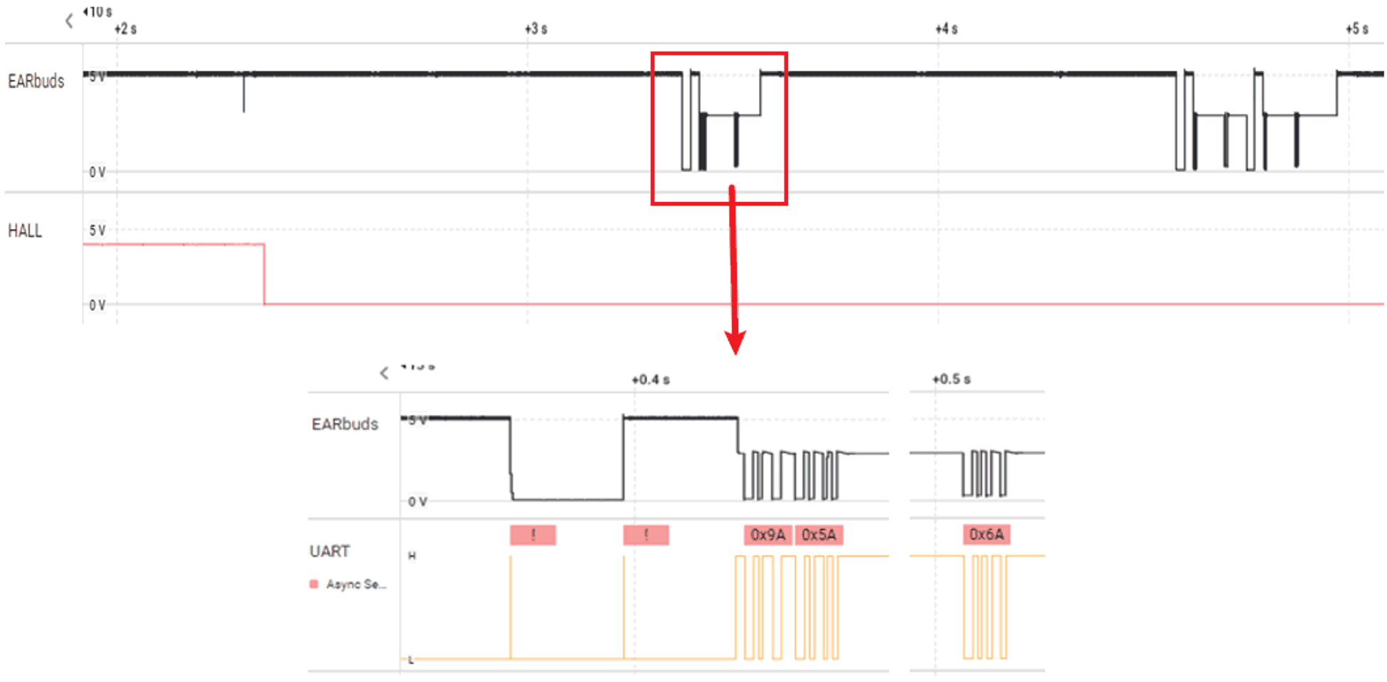
The charging and communication between the earbuds and the cradle happen on a single line. For example, Figure 4-1 shows the communication and charging waveforms from a third-party TWS earbud. The red line shows the output of the hall sensor, and the voltage drop indicates the lid closing. The black line is measured at the right ear pogo pin. The orange line shows the digital information contained in the black line decoded using UART protocol, 1200 baud rate. When charging the earbuds, the Pogo pin is working at 5V. However, when the TWS cradle tries to communicate with the earbuds, the logic high is 3.3V.
 Figure 4-1 Waveforms From a Third-Party
TWS Earbud
Figure 4-1 Waveforms From a Third-Party
TWS EarbudIt can be seen that by default, the Pogo pin is 5V and is charging the earbuds. with the lid closing, the TWS case sends a fixed 5V-0 V-5V pattern to indicate the start of a command. Then the case sends 0x9A5A and the earbuds respond with 0x6A.
The pattern and design above are for reference only, the customer can customize their communication and power logic, and the TWS case can send customized commands/information to the earbuds, for example, case battery percentage, earbuds/case SN, charging status, and so forth.
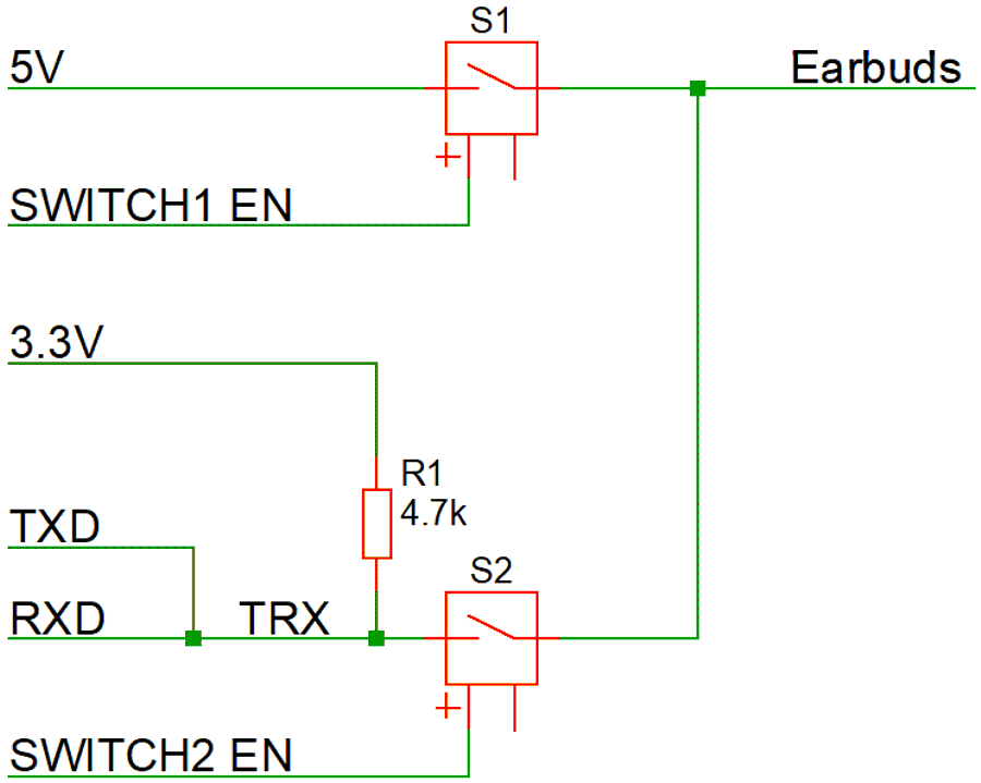
Figure 4-2 shows reference power and the communication design based on MSPM0.
 Figure 4-2 Reference Power and
Communication Design Based on MSPM0
Figure 4-2 Reference Power and
Communication Design Based on MSPM0As shown in Figure 4-2, switches S1 and S2 control when to charge the earbuds and when to start the communication. When S1 is closed and S2 is open, the cradle charges the earbuds, and when S2 is closed and S1 is open, the cradle can communicate with the earbuds with a 3.3V logic high.
As mentioned before, the MSPM0L series supports two UART peripherals, hence it can communicate with the left and right earbuds simultaneously. The corresponding design can be seen in the figure below. In this design, four switches are used to control the left and right earbuds separately, this is ideal for applications where a great amount of information needs to be transformed.
 Figure 4-3 Reference Design 1
However, to save costs and resources, the following designs can also be used:
 Figure 4-4 Reference Design 2
 Figure 4-5 Reference Design 3
In Figure 4-4, the left and right earbuds share the same MSPM0 UART peripheral. Hence, they cannot communicate with the TWS case simultaneously, but they still share separate communication lines. While in Figure 4-5, the Pogo pins of the left and right earbuds are connected together, meaning they will receive the same message. This is like I2C communication where the TWS case is the master device and two earbuds are slave devices, and they share the same data line.