SLAAEI7 December 2023 MSPM0G3507
3 Signal Chain
This section presents leveraging the capable analog peripherals of the MSPM0 microcontroller series to adjust for challenges of pressure transmitter designs and other high-gain sensor interfaces. A significant amplification of the signal is necessary to scale a single-digit mV signal from a sensor to the full scale input of an ADC. This amplification is not solely achievable with the internal operational amplifiers of the MSPM0. Therefore, an INA350 instrumentation amplifier, with 50x amplification, is used as the first stage of the signal chain. The following amplification is handled by the internal chopper-stabilized OPA of the MSPM0, which is internally connected to the ADC of the MSPM0. The internal OPA, therefore, allows for flexibility in amplification between 50x (OPA in a buffer configuration without amplification) and 1600x with the internal OPA setting at 32x amplification. The signal chain is visualized in Figure 3-1.
 Figure 3-1 Signal Chain Using INA350 and MSPM0 Internal OPA
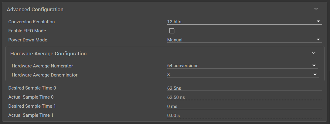
The ADC is used in oversampling mode to improve the effective resolution by utilizing the hardware assisted averaging feature. The ADC is configured to aggregate 64 samples in the result buffer and then the result is divided by the factor of 8, which is done by right shifting by 3 bits in hardware. This configuration is done directly in the SysConfig tool as displayed in Figure 3-2. The total conversion time for a sample is 64 times the sample time, and conversion time, per sample because the sample time configured in SysConfig always equates to one single sample. The conversion time is dependent on the clock that the ADC is sourced from. Aggregating 64 samples and dividing the resulting sum by 8 increases the nominal resolution of the ADC by 3 bits when considering Equation 1.
 Figure 3-2 SysConfig ADC Configurations Settings for Oversampling
Depending on the size and resolution requirements for a specific application this setup offers the flexibility to use either the internal reference voltage generation of the MSPM0 or an external voltage reference.
Tests results explained in Section 4 were conducted using LP-MSPM0G3507 LaunchPad™ Development Kit and a cost-optimized REF29x voltage reference, which outputs 2.5 V to the MSPM0G3507 and 2.5 V to the INA350.
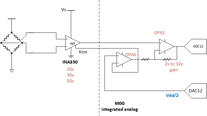
Figure 3-3 shows the complete option for a bipolar bridge input. Processing a bipolar input using a single-supply signal chain requires a DC shift added to the input, starting with adding Vcm to the INA350 output. Once a DC shift is added, the rest of the signal chain needs to take the DC shift into account for further amplification. The next stage is converted from a simple gain stage into a difference amplifier.
The difference amplifier implements using the two amplifiers shown in Figure 3-3. This implementation has multiple advantages. First, the difference amplifier provides high-impedance on both positive and negative inputs. Second, the amplifier allows using the buffered second input (which is the Vcm) as an output to feed the INA350 reference node. The negative input for the OPA is generated using the internal low resolution 8-bit DAC or the high resolution DAC12 (Figure 3-3).
Offset calibration is also activated in Figure 3-3. This activation is done by measuring the ADC12, in case of zero input, and then adjusting the DAC12 output, until the ADC12 is reading zero value (the bipolar input is represented by mid-scale reading). This offset calibration compensates for combined offset of the whole signal chain.
 Figure 3-3 Bipolar High-Gain Signal Chain Using the Internal DAC