SLAAEM1 June 2024 MSPM0C1104 , MSPM0C1104 , MSPM0L1105 , MSPM0L1105
3.4 Main Controller Circuit
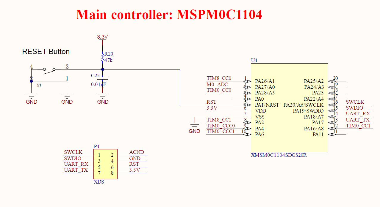
The peripheral circuit of the MSPM0C1104 mainly consists of the reset circuit and the program burning interfaces, as shown in Figure 3-5.
In this solution, the assignment of pin functions for MSPM0C1104 can refer to Table 3-1. TIM0_CC0 and TIM0_CCC0 are complementary PWM signals, and TIM0_CC1 and TIM0_CCC1 are complementary PWM signals. Reserving the UART interface is for convenient debugging and only four signals are required for burning, including SWCLK, SWDIO, RST and GND.
 Figure 3-5 Main Controller
Circuit
Figure 3-5 Main Controller
CircuitTable 3-1 Hardware Connection
| Connection Type | Connection Net | LP-MSPM0LC1104 Pin Number: Pin Name |
|---|---|---|
| Power supply input | 3.3V | Pin 6: VDD |
| GND | Pin 7: VSS | |
| PWM output | TIM0_CC0 | Pin 3: PA28 |
| TIM0_CCC0 | Pin 9: PA4 | |
| TIM0_CC1 | Pin 12: PA16 | |
| TIM0_CCC1 | Pin 10: PA6 | |
| ADC input | M0_ADC | Pin 2: PA27 |
| Encoder input | TIM8_CC0 | Pin 1: PA26 |
| TIM8_CC1 | Pin 8: PA2 | |
| Program burning interfaces | SWCLK | Pin 16: PA20 |
| SWDIO | Pin 15: PA19 | |
| UART_RX | Pin 14: PA18 | |
| UART_TX | Pin 13: PA17 | |
| RST | Pin 5: PA1 |