SLAAEO3 September 2024 MSPM0L2227 , MSPM0L2228
4.4.1 LCD Memory Organization
User software selects which segments are on or off by using the LCD memory registers. Each bit represents a single LCD segment connected to a COMx and Sx pin pair. The row (or byte) corresponds to the Sx pin, and the columns (or each bit within the byte) correspond to the COMx pins. In 2-mux through 4-mux modes, the upper and lower nibbles of each row correspond to different Sx pins. In this case, only up to 4 bits in the byte are needed since there are only up to 4 COMx lines, so a single byte sets two Sx pins. In 5-mux through 8-mux modes, there are more than 4 COMx lines so the whole row (byte) is required for each segment Sx pin.
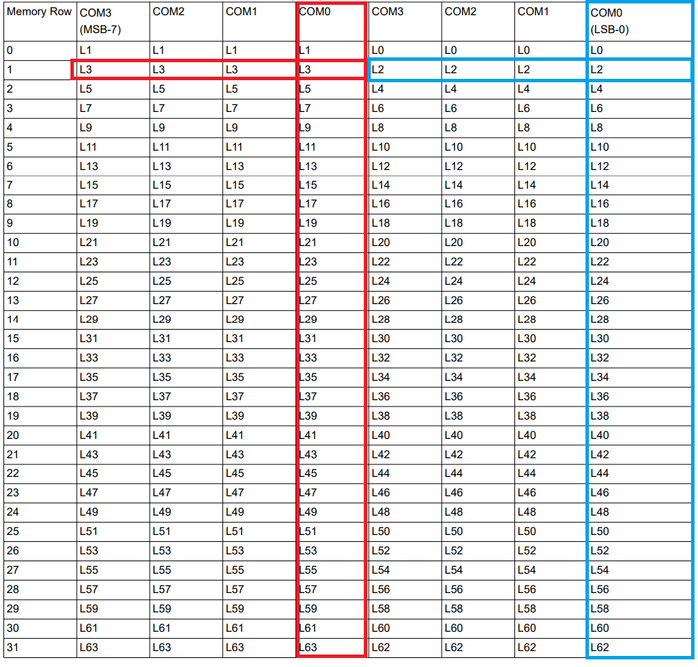
Figure 4-7 shows an example memory configuration for 4-mux mode. The L2 and L3 segment pins in this example correspond to the lower and upper nibbles of the byte at LCD memory offset 1. To control the segment connected to COM0 + L2 or COM0 + L3, the software sets the highlighted bits to either 1 or 0 to indicate the desired LCD segment state "on" or "off."
 Figure 4-7 LCD Memory Map Example