SLAAEO8 October 2024 MSPM0C1103 , MSPM0C1103-Q1 , MSPM0C1104 , MSPM0C1104-Q1 , MSPM0G1105 , MSPM0G1106 , MSPM0G1107 , MSPM0G1505 , MSPM0G1506 , MSPM0G1507 , MSPM0G3105 , MSPM0G3105-Q1 , MSPM0G3106 , MSPM0G3106-Q1 , MSPM0G3107 , MSPM0G3107-Q1 , MSPM0G3505 , MSPM0G3505-Q1 , MSPM0G3506 , MSPM0G3506-Q1 , MSPM0G3507 , MSPM0G3507-Q1 , MSPM0G3519 , MSPM0L1105
4.1 ADC Configuration of MSPM0
- Clock
 Figure 4-1 ADC Clock Sysconfig
Configuration
Figure 4-1 ADC Clock Sysconfig
Configuration- ADC Clock(ADCCLK)
- SYSOSC(max 32MHz)
- HFCLK(max 48MHz)
- ULPCLK(max 40MHz, PD0)
- ADC Sampling Clock(SAMPCLK):divided by ADCCLK
- Conversion
Clock(Conversion clock):ADC IP internal 80MHz crystal oscillator
- The conversion time for 12-bit ADC data is approximately 14 conversion clock cycles
- ADC Clock(ADCCLK)
- Sampling mode
 Figure 4-2 ADC Sampling Mode
Sysconfig Configuration
 - Conversion mode
- Single conversion: Only a single point is converted during each sampling and conversion process, and the MEMCTL number used is determined by configuring the conversion start address STARTADD;
- Sequence conversion: By defining the starting address STARTADD and ending address ENDADD of the MEMCTL number used for conversion, a sequence of data conversion can be defined (MEMCTL0-11 corresponds to MEMRES0-11), and ADC channels can be configured separately for each MEMCTLx;
- Enable repeat mode
- Non-repetitive mode: After each round of conversion is completed, conversion enable bit (ENC) automatically resets to zero;
- Repetitive mode: The conversion process will continue to be enabled until the conversion enable bit (ENC) is cleared by the software;
- Sampling trigger source
- Software: Software setting CTL1.SC bit trigger sampling;
- Event: Event rising edge triggering sampling;
- Sampling mode
- Automatic sampling: After the sampling trigger signal is generated, the sampling signal SAMPLE is automatically raised, with a sampling time of several SAMPCLK clock cycles defined by SCOMP;
- Manual sampling (only supports software triggering, does not support repetitive mode and sequence conversion, does not support hardware oversampling): The sampling signal SAMPLE is synchronized pulling up with the software triggering signal CTL1.SC. The sampling time is determined by determining the pulling up time of the SC, and triggering and sampling are completed synchronously;
- Trigger mode
- In the repetition and sequence conversion modes, the trigger mode (TRIG) needs to be selected to determine whether the next round of conversion requires a trigger signal.
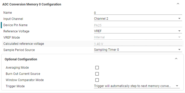
- Conversion memory configuration
 Figure 4-3 ADC Conversion Memory
Sysconfig Configuration
 - The amount of conversion memory
that needs to be configured is determined by the MEMCTL start and end numbers
defined in the conversion mode:
- Sampling input channel
- Reference voltage
- VDDA:Internal power supply (3.3V)
- VREF
- Internal:2.5V/1.4V
- External:0~3.3V
Sampling Timer Source: Select the timer used for sampling time counting in automatic sampling mode
- Others
- Oversampling
- sampling result multiple = number of sampling points/average denominator
- Interrupt
- Not using DMA: enable MEMx result loading interrupt, and read data in the interrupt after each sampling result is generated;
- Using DMA: Enable DMA completion interrupts, and trigger DMA data transfer based on the ADC MEMx result loading, and set the amount of DMA transfer data. Once the DMA transfer is completed, enter DMA interrupts to process ADC sampling data at once.
- Oversampling