SLAS638A
January 2009 – October 2015
SN65HVS885
PRODUCTION DATA.
1
Features
2
Applications
3
Description
4
Revision History
5
Pin Configuration and Functions
6
Specifications
6.1
Absolute Maximum Ratings
6.2
ESD Ratings
6.3
Recommended Operating Conditions
6.4
Thermal Information
6.5
Electrical Characteristics
6.6
Timing Requirements
6.7
Switching Characteristics
6.8
Typical Characteristics
7
Parameter Measurement Information
7.1
Waveforms
7.2
Signal Conventions
8
Detailed Description
8.1
Overview
8.2
Functional Block Diagram
8.3
Feature Description
8.3.1
Digital Inputs
8.3.2
Debounce Filter
8.3.3
Shift Register
8.3.4
Temperature Sensor
8.4
Device Functional Modes
9
Application and Implementation
9.1
Application Information
9.1.1
System-Level EMC
9.1.2
Input Channel Switching Characteristics
9.1.3
Digital Interface Timing
9.1.4
Cascading for High Channel Count Input Modules
9.2
Typical Application
9.2.1
Design Requirements
9.2.2
Detailed Design Procedure
9.2.2.1
Input Stage
9.2.2.2
Setting Debounce Time
9.2.2.3
Using the HOT Indicator
9.2.2.4
Example: High-Voltage Sensing Application
9.2.3
Application Curve
10
Power Supply Recommendations
11
Layout
11.1
Layout Guidelines
11.2
Layout Example
12
Device and Documentation Support
12.1
Community Resources
12.2
Trademarks
12.3
Electrostatic Discharge Caution
12.4
Glossary
13
Mechanical, Packaging, and Orderable Information
11 Layout
11.1 Layout Guidelines
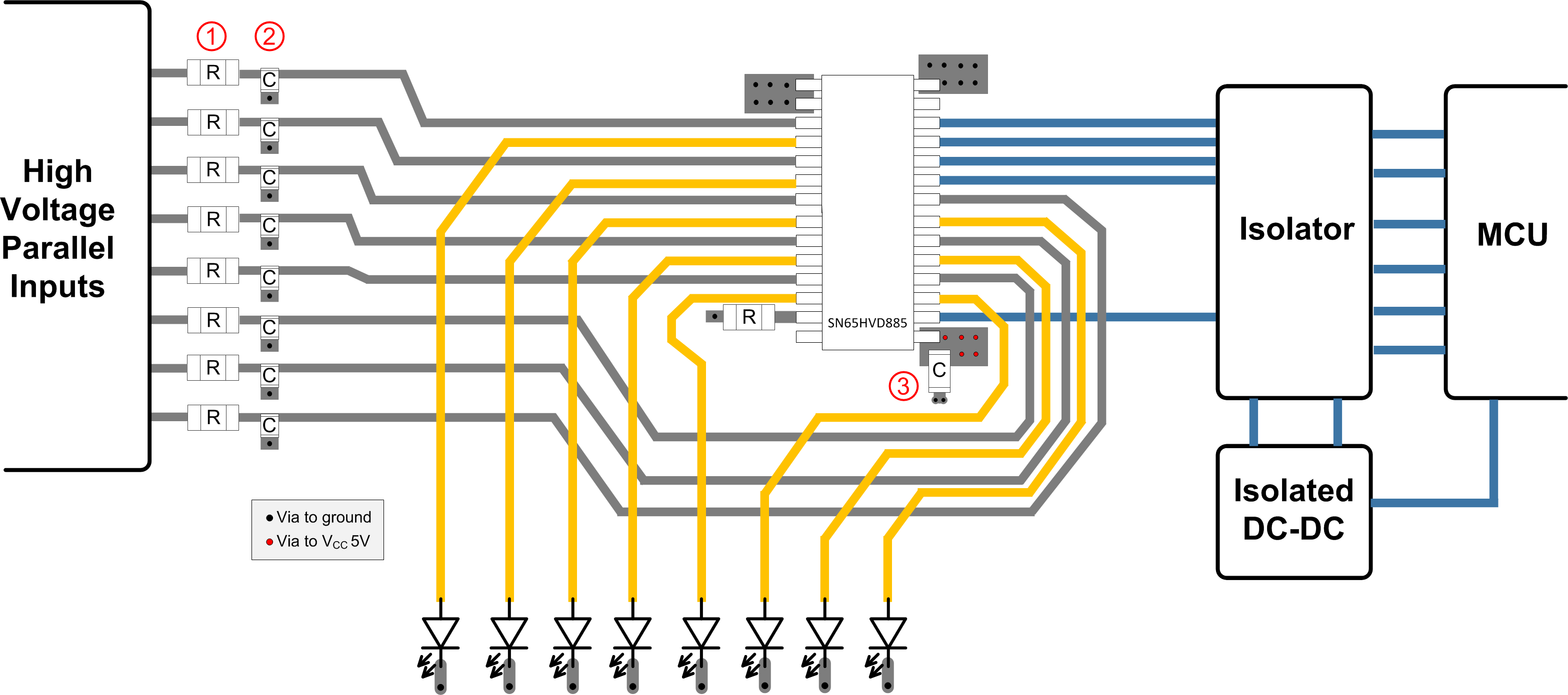
Place series MELF resistors between the field inputs and the device input pins.
Place small ~22 nF capacitors close to the field input pins to reduce noise.
Place a supply buffering 0.1-µF capacitor around as close to the V
CC
pin as possible.
11.2 Layout Example