SLAS715D June 2010 – October 2024 TLV320AIC3104-Q1
PRODUCTION DATA
- 1
- 1 Features
- 2 Applications
- 3 Description
- 4 Device Comparison
- 5 Pin Configuration and Functions
-
6 Specifications
- 6.1 Absolute Maximum Ratings
- 6.2 ESD Ratings
- 6.3 Recommended Operating Conditions
- 6.4 Thermal Information
- 6.5 Electrical Characteristics
- 6.6 Switching Characteristics I2S/LJF/RJF Timing in Master Mode
- 6.7 Switching Characteristics I2S/LJF/RJF Timing in Slave Mode
- 6.8 Switching Characteristics DSP Timing in Master Mode
- 6.9 Switching Characteristics DSP Timing in Slave Mode
- 6.10 Typical Characteristics
-
7 Detailed Description
- 7.1 Overview
- 7.2 Functional Block Diagram
- 7.3
Feature Description
- 7.3.1 Audio Data Converters
- 7.3.2 Stereo Audio ADC
- 7.3.3 Automatic Gain Control (AGC)
- 7.3.4 Stereo Audio DAC
- 7.3.5 Digital Audio Processing for Playback
- 7.3.6 Digital Interpolation Filter
- 7.3.7 Delta-Sigma Audio DAC
- 7.3.8 Audio DAC Digital Volume Control
- 7.3.9 Analog Output Common-mode Adjustment
- 7.3.10 Audio DAC Power Control
- 7.3.11 Audio Analog Inputs
- 7.3.12 Analog Input Bypass Path Functionality
- 7.3.13 ADC PGA Signal Bypass Path Functionality
- 7.3.14 Input Impedance and VCM Control
- 7.3.15 MICBIAS Generation
- 7.3.16 Analog Fully Differential Line Output Drivers
- 7.3.17 Analog High-Power Output Drivers
- 7.3.18 Short-Circuit Output Protection
- 7.3.19 Jack and Headset Detection
- 7.4 Device Functional Modes
- 7.5 Programming
- 8 Register Maps
- 9 Application and Implementation
- 10Device and Documentation Support
- 11Revision History
- 12Mechanical, Packaging, and Orderable Information
7.3.3 Automatic Gain Control (AGC)
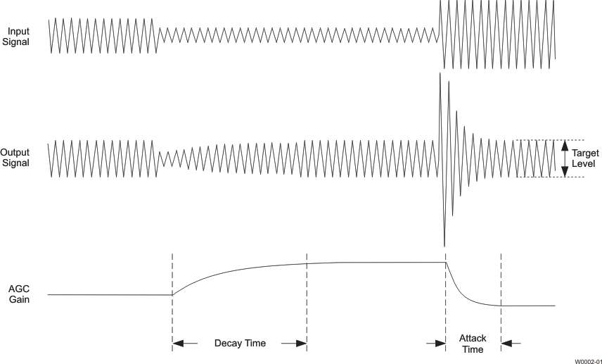
An automatic gain control (AGC) circuit is included with the ADC and can be used to maintain nominally constant output signal amplitude when recording speech signals (the AGC can be fully disabled if not needed). This circuitry automatically adjusts the PGA gain when the input signal becomes overly loud or very weak, such as when a person speaking into a microphone moves closer or farther from the microphone. The AGC algorithm has several programmable settings, including target level, attack and decay time constants, noise threshold, and maximum PGA gain applicable that allow the algorithm to be fine-tuned for any particular application. These AGC features are explained in this section, and Figure 7-1 illustrates their operation. The algorithm uses the absolute average of the signal (which is the average of the absolute value of the signal) as a measure of the nominal amplitude of the output signal.
The TLV320AIC3104-Q1 allows programming of eight different target levels, which can be programmed from –5.5 dB to –24 dB relative to a full-scale signal. Because the device reacts to the signal absolute average and not to peak levels, it is recommended that the target level be set with enough margin to avoid clipping at the occurrence of loud sounds.
Attack can be varied from 7 ms to 1,408 ms. The extended right-channel attack time can be programmed by writing to page 0, register 103, and the left channel is programmed by writing to page 0, register 105.
Decay time can be varied in the range from 0.05 s to 22.4 s. The extended right-channel decay time can be programmed by writing to page 0, register 104, and the left channel is programmed by writing to page 0, register 106.
The actual AGC decay time maximum is based on a counter length, so the maximum decay time scales with the clock setup that is used. Table 7-1 shows the relationship of the NCODEC ratio to the maximum time available for the AGC decay. In practice, these maximum times are extremely long for audio applications and should not limit any practical AGC decay time that is needed by the system.
| NCODEC RATIO | MAXIMUM DECAY TIME (SECONDS) |
|---|---|
| 1 | 4 |
| 1.5 | 5.6 |
| 2 | 8 |
| 2.5 | 9.6 |
| 3 | 11.2 |
| 3.5 | 11.2 |
| 4 | 16 |
| 4.5 | 16 |
| 5 | 19.2 |
| 5.5 | 22.4 |
| 6 | 22.4 |
In this situation, the AGC considers the input signal as a silence and will set the noise threshold flag while reducing the gain down to 0 dB in steps of 0.5 dB every sample period. The gain stays at 0 dB unless the input speech signal average rises above the noise threshold setting. This ensures that noise does not get gained up in the absence of speech. Noise threshold level in the AGC algorithm is programmable from –30 dB to –90 dB relative to full scale. A disable noise gate feature is also available. This operation includes programmable debounce and hysteresis functionality to avoid the AGC gain from cycling between high gain and 0 dB when signals are near the noise threshold level. When the noise threshold flag is set, the status of gain applied by the AGC and the saturation flag should be ignored.
The Maximum PGA gain applicable can be set by the user, which restricts the maximum PGA gain that can be applied by the AGC algorithm. This can be used for limiting PGA gain in situations where environmental noise is greater than programmed noise threshold. It can be programmed from 0 dB to 59.5 dB in steps of 0.5 dB.
 Figure 7-1 Typical Operation of the AGC Algorithm During Speech Recording
The actual AGC decay time maximum is based on a counter length, so the maximum decay time scales with the clock setup that is used. Table 7-1 shows the relationship of the NCODEC ratio to the maximum time available for the AGC decay. In practice, these maximum times are extremely long for audio applications and should not limit any practical AGC decay time that is needed by the system.