SLAS763C August   2012  – October 2018 PCM5121 , PCM5122

PRODUCTION DATA.  

  1. Features
  2. Applications
  3. Description
    1.     Device Images
      1.      Simplified System Diagram
  4. Revision History
  5. Device Comparison
  6. Pin Configuration and Functions
    1. 6.0.1 RHB Package I2C Mode (MODE1 tied to DGND and MODE2 tied to DVDD) Top View
    2. 6.0.2 RHB Package SPI Mode (MODE1 tied to DVDD) Top View
    3. 6.0.3 RHB Package Hardwired Mode (MODE1 tied to DGND, MODE2 tied to DGND) Top View
    4.     Pin Functions
  7. Specifications
    1. 7.1 Absolute Maximum Ratings
    2. 7.2 ESD Ratings
    3. 7.3 Recommended Operating Conditions
    4. 7.4 Thermal Information
    5. 7.5 Electrical Characteristics
    6. 7.6 Timing Requirements: SCK Input
    7. 7.7 Timing Requirements: XSMT
    8. 7.8 Switching Characteristics
    9. 7.9 Typical Characteristics
  8. Detailed Description
    1. 8.1 Overview
    2. 8.2 Functional Block Diagram
    3. 8.3 Feature Description
      1. 8.3.1 Terminology
      2. 8.3.2 Audio Data Interface
        1. 8.3.2.1 Audio Serial Interface
        2. 8.3.2.2 PCM Audio Data Formats
        3. 8.3.2.3 Zero Data Detect
      3. 8.3.3 XSMT Pin (Soft Mute / Soft Un-Mute)
      4. 8.3.4 Audio Processing
        1. 8.3.4.1 PCM512x Audio Processing
          1. 8.3.4.1.1 Overview
          2. 8.3.4.1.2 Software
        2. 8.3.4.2 Interpolation Filter
        3. 8.3.4.3 Fixed Audio Processing Flow (Program 5)
          1. 8.3.4.3.1 Filter Programming Changes
          2. 8.3.4.3.2 Processing Blocks – Detailed Descriptions
          3. 8.3.4.3.3 Biquad Section
          4. 8.3.4.3.4 Dynamic Range Compression
          5. 8.3.4.3.5 Stereo Mixer
          6. 8.3.4.3.6 Stereo Multiplexer
          7. 8.3.4.3.7 Mono Mixer
          8. 8.3.4.3.8 Master Volume Control
          9. 8.3.4.3.9 Miscellaneous Coefficients
      5. 8.3.5 DAC Outputs
        1. 8.3.5.1 Analog Outputs
        2. 8.3.5.2 Recommended Output Filter for the PCM512x
        3. 8.3.5.3 Choosing Between VREF and VCOM Modes
          1. 8.3.5.3.1 Voltage Reference and Output Levels
          2. 8.3.5.3.2 Mode Switching Sequence, from VREF Mode to VCOM Mode
        4. 8.3.5.4 Digital Volume Control
          1. 8.3.5.4.1 Emergency Ramp-Down
        5. 8.3.5.5 Analog Gain Control
      6. 8.3.6 Reset and System Clock Functions
        1. 8.3.6.1 Clocking Overview
        2. 8.3.6.2 Clock Slave Mode With Master and System Clock (SCK) Input (4 Wire I2S)
        3. 8.3.6.3 Clock Slave Mode With BCK PLL to Generate Internal Clocks (3-Wire PCM)
        4. 8.3.6.4 Clock Generation Using the PLL
        5. 8.3.6.5 PLL Calculation
          1. 8.3.6.5.1 Examples:
            1. 8.3.6.5.1.1 Recommended PLL Settings
        6. 8.3.6.6 Clock Master Mode from Audio Rate Master Clock
        7. 8.3.6.7 Clock Master from a Non-Audio Rate Master Clock
    4. 8.4 Device Functional Modes
      1. 8.4.1 Choosing a Control Mode
        1. 8.4.1.1 Software Control
          1. 8.4.1.1.1 SPI Interface
            1. 8.4.1.1.1.1 Register Read and Write Operation
          2. 8.4.1.1.2 I2C Interface
            1. 8.4.1.1.2.1 Slave Address
            2. 8.4.1.1.2.2 Register Address Auto-Increment Mode
            3. 8.4.1.1.2.3 Packet Protocol
            4. 8.4.1.1.2.4 Write Register
            5. 8.4.1.1.2.5 Read Register
            6. 8.4.1.1.2.6 Timing Characteristics
      2. 8.4.2 VREF and VCOM Modes
    5. 8.5 Programming
  9. Application and Implementation
    1. 9.1 Application Information
    2. 9.2 Typical Application
      1. 9.2.1 Design Requirements
      2. 9.2.2 Detailed Design Procedure
      3. 9.2.3 Application Curve
  10. 10Power Supply Recommendations
    1. 10.1 Power Supply Distribution and Requirements
    2. 10.2 Recommended Powerdown Sequence
      1. 10.2.1 XSMT = 0
      2. 10.2.2 Clock Error Detect
      3. 10.2.3 Planned Shutdown
      4. 10.2.4 Unplanned Shutdown
    3. 10.3 External Power Sense Undervoltage Protection Mode
    4. 10.4 Power-On Reset Function
      1. 10.4.1 Power-On Reset, DVDD 3.3-V Supply
      2. 10.4.2 Power-On Reset, DVDD 1.8-V Supply
    5. 10.5 PCM512x Power Modes
      1. 10.5.1 Setting Digital Power Supplies and I/O Voltage Rails
      2. 10.5.2 Power Save Modes
      3. 10.5.3 Power Save Parameter Programming
  11. 11Layout
    1. 11.1 Layout Guidelines
    2. 11.2 Layout Example
  12. 12Register Maps
    1. 12.1 PCM512x Register Map
      1. 12.1.1 Detailed Register Descriptions
        1. 12.1.1.1 Register Map Summary
        2. 12.1.1.2 Page 0 Registers
        3. 12.1.1.3 Page 1 Registers
        4. 12.1.1.4 Page 44 Registers
        5. 12.1.1.5 Page 253 Registers
      2. 12.1.2 PLL Tables for Software Controlled Devices
      3. 12.1.3 Coefficient Data Formats
      4. 12.1.4 Power Down and Reset Behavior
  13. 13Device and Documentation Support
    1. 13.1 Development Support
    2. 13.2 Documentation Support
    3. 13.3 Related Links
    4. 13.4 Receiving Notification of Documentation Updates
    5. 13.5 Community Resources
    6. 13.6 Trademarks
    7. 13.7 Electrostatic Discharge Caution
    8. 13.8 Glossary
  14. 14Mechanical, Packaging, and Orderable Information

Clock Master Mode from Audio Rate Master Clock

In Master Mode, the device generates bit clock (BCK) and left-right clock (LRCK) and outputs them on the appropriate pins. To configure the device in this mode, first put the device into reset, then use registers BCKO and LRKO (Pg 0, Reg 9 0x09). Then reset the LRCK and BCK divider counters using bits RBCK and RLRK (Pg 0, Reg 12 0x0C). Finally, exit reset.

An example of this is given in register programming examples in the PCM5242 data sheet (SLASE12.)

Figure 64 shows a simplified serial port clock tree for the device in master mode.
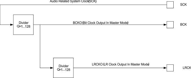
PCM5121 PCM5122 f_pcm51xx_serialport_clk_tree.gifFigure 64. Simplified Clock Tree for SCK Sourced Master Mode

In master mode, SCK is an input and BCK/LRCK are outputs. BCK and LRCK are integer divisions of SCK. Master mode with a non-audio rate master clock source will require external GPIOs to use the PLL in standalone mode.

The PLL will also need to be configured to ensure that the onchip audio processor processor can be driven at its maximum clock rate.

Register changes that need to be done include switching the device into master mode, and setting the divider ratio.

Here is an example of using 24.576 MCLK as a master clock source and driving the BCK and LRCK with integer dividers to create 48 kHz.

In this mode, the DAC section of the device is also running from the PLL output. While the PLL inside the PCM512x is one that has been specified to achieve the stated performance, using the SCK CMOS Oscillator source will have less jitter.

To switch the DAC clocks (SDAC in the Figure 63) the following registers should be modified.

  • Clock Tree Flex Mode (Page 253, Registers 0x3F and 0x40)
  • DAC and OSR Source Clock Register (Page 0, Reg 14) – set to 0x30 (SCK input, and OSR is set to whatever the DAC source is)
  • The DAC clock divider should be 16 FS.
    • 16 × 48 kHz = 768 kHz
    • 24.576 MHz (SCK in) / 768 kHz = 32
    • Therefor, divide ratio for register DDAC (Page 0, Reg 28 0x1C) should be set to 32. The may the register is mapped gives 0x00 = 1, so 32 must be converted to 0x1F.

An example configuration can be found in the PCM5242 data sheet (SLASE12).