SLAS901C December   2016  – January 2021 HD3SS213

PRODUCTION DATA  

  1. Features
  2. Applications
  3. Description
  4. Revision History
  5. Pin Configuration and Functions
  6. Specifications
    1. 6.1 Absolute Maximum Ratings
    2. 6.2 ESD Ratings
    3. 6.3 Recommended Operating Conditions
    4. 6.4 Thermal Information
    5. 6.5 Electrical Characteristics
    6. 6.6 Timing Requirements
    7. 6.7 Typical Characteristics
  7. Detailed Description
    1. 7.1 Overview
    2. 7.2 Functional Block Diagram
    3. 7.3 Feature Description
    4. 7.4 Device Functional Modes
  8. Application and Implementation
    1. 8.1 Application Information
    2. 8.2 Typical Applications
      1. 8.2.1 HD3SS213 AUX Channel in 2:1 Application
        1. 8.2.1.1 Design Requirements
        2. 8.2.1.2 Detailed Design Procedure
        3. 8.2.1.3 Application Curves
      2. 8.2.2 HD3SS213 AUX Channel in 1:2 Application
  9. Layout
    1. 9.1 Layout Guidelines
      1. 9.1.1 Differential Traces
    2. 9.2 Layout Example
  10. 10Device and Documentation Support
    1. 10.1 Receiving Notification of Documentation Updates
    2. 10.2 Support Resources
    3. 10.3 Trademarks
    4. 10.4 Electrostatic Discharge Caution
    5. 10.5 Glossary
  11. 11Mechanical, Packaging, and Orderable Information

HD3SS213 AUX Channel in 1:2 Application

AUX channel is controlled by AUX_SEL. This pin configures the switch to route the incoming AUX signal to the outgoing AUX path, when AUX_SEL = 0 the AUXA channel is routed to AUXC, when AUX_SEL = 1 the AUXB channel is routed to AUXC.
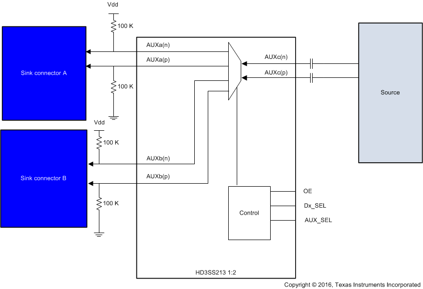
GUID-BEC263F2-67BC-4190-AF2E-4AA156C7DCD5-low.gifFigure 8-8 HD3SS213 AUX Channel in 1:2 Application Schematic