The Texas Instruments Dynamic NFC Interface Transponder RF430CL330H is an NFC Tag Type 4 device that combines a wireless NFC interface and a wired SPI or I2C interface to connect the device to a host. The NDEF message in the SRAM can be written and read from the integrated SPI or I2C serial communication interface and can also be accessed and updated wirelessly through the integrated ISO14443B-compliant RF interface that supports up to 848 kbps.
This operation allows NFC connection handover for an alternative carrier like Bluetooth, Bluetooth Low Energy (BLE), and Wi-Fi as an easy and intuitive pairing process or authentication process with only a tap. As a general NFC interface, the RF430CL330H enables end equipments to communicate with the fast-growing infrastructure of NFC-enabled smart phones, tablets, and notebooks.
PART NUMBER | PACKAGE | BODY SIZE(2) |
---|---|---|
RF430CL330HPW | TSSOP (14) | 5 mm x 4.4 mm |
RF430CL330HRGT | VQFN (16) | 3 mm x 3 mm |
Figure 1-1 shows a typical application diagram for the RF430CL330H device.
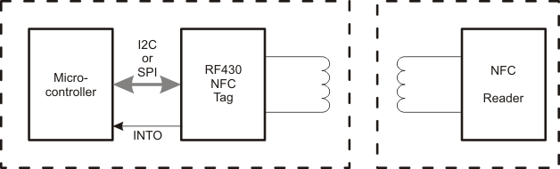
Figure 3-1 shows the pin assignments for the PW package.
Figure 3-2 shows the pin assignments for the RGT package.
TERMINAL | I/O | DESCRIPTION | ||
---|---|---|---|---|
NAME | NO. | |||
PW | RGT | |||
VCC | 1 | 15 | PWR |
3.3-V power supply |
ANT1 | 2 | 1 | RF |
Antenna input 1 |
ANT2 | 3 | 2 | RF |
Antenna input 2 |
RST | 4 | 3 | I |
Reset input (active low) |
E0 (TMS) | 5 | 4 | I |
I2C address select 0 SPI mode select 0 (JTAG test mode select) |
E1 (TDO) | 6 | 5 | I (O) |
I2C address select 1 SPI mode select 1 (JTAG test data output) |
E2 (TDI) | 7 | 6 | I |
I2C address select 2 (JTAG test data in) |
INTO (TCK) | 8 | 7 | O |
Interrupt output (JTAG test clock) |
SCMS/ CS |
9 | 8 | I |
Serial Communication Mode Select (during device initialization) Chip select (in SPI mode) |
SCK | 10 | 9 | I |
SPI clock input (SPI mode) |
SO/SCL | 11 | 10 | I/O |
SPI slave out (SPI mode) I2C clock (I2C mode) |
SI/SDA | 12 | 11 | I/O |
SPI slave in (SPI mode) I2C data (I2C mode) |
VCORE | 13 | 12 | PWR |
Regulated core supply voltage |
VSS | 14 | 13 | PWR |
Ground supply |
NC | - | 14, 16 | Leave open, No connection |
MIN | MAX | UNIT | |
---|---|---|---|
Voltage applied at VCC referenced to VSS (VAMR) | -0.3 | 4.1 | V |
Voltage applied at VANT referenced to VSS (VAMR) | -0.3 | 4.1 | V |
Voltage applied to any pin (references to VSS) | -0.3 | VCC + 0.3 | V |
Diode current at any device pin | ±2 | mA |
MIN | MAX | UNIT | ||
---|---|---|---|---|
Tstg | Storage temperature range(3) | -40 | 125 | °C |
MIN | NOM | MAX | UNIT | ||
---|---|---|---|---|---|
VCC | Supply voltage during program execution no RF field present | 3.0 | 3.3 | 3.6 | V |
Supply voltage during program execution with RF field present | 2.0 | 3.3 | 3.6 | V | |
VSS | Supply voltage (GND reference) | 0 | V | ||
TA | Operating free-air temperature | -40 | 85 | °C | |
C1 | Decoupling capacitor on VCC(1) | 0.1 | µF | ||
C2 | Decoupling capacitor on VCC(1) | 1 | µF | ||
CVCORE | Capacitor on VCORE(1) | 0.1 | 0.47 | 1 | µF |
MIN | NOM | MAX | UNIT | ||
---|---|---|---|---|---|
fc | Carrier frequency | 13.56 | MHz | ||
VANT_peak | Antenna input voltage | 3.6 | V | ||
Z | Impedance of LC circuit | 6.5 | 15.5 | kΩ | |
LRES | Coil inductance(2) | 2.66 | µH | ||
CRES | Total resonance capacitance(2) CRES = CIN+CTune | 51.8 | pF | ||
CTune | External resonance capacitance | CRES – CIN(1) | pF | ||
QT | Tank quality factor | 30 |
PARAMETER | TEST CONDITIONS | VCC | MIN | TYP | MAX | UNIT | |
---|---|---|---|---|---|---|---|
ICC(SPI) | SPI, fSCK,MAX, SO = Open, Writing into NDEF memory | 3.3 V | 250 | µA | |||
ICC(I2C) | I2C, 400 kHz, Writing into NDEF memory | 3.3 V | 250 | µA | |||
ICC(RF enabled) | RF enabled, no RF field present | 3.3 V | 40 | µA | |||
ICC(Inactive) | Standby enable = 0, RF disabled, no serial communication | 3.3 V | 15 | µA | |||
ICC(Standby) | Standby enable = 1, RF disabled, no serial communication | 3.3 V | 10 | 45 | µA | ||
ΔICC(StrongRF) | Additional current consumption with strong RF field present | 3.0 V to 3.6 V | 160 | µA | |||
ICC(RF,lowVCC) | Current drawn from VCC < 3.0 V with RF field present (passive operation) | 2.0 V to 3.0 V | 0 | µA |
PARAMETER | TEST CONDITIONS | VCC | MIN | TYP | MAX | UNIT | |
---|---|---|---|---|---|---|---|
VIL | Low-level input voltage | 0.3× VCC | V | ||||
VIH | High-level input voltage | 0.7× VCC | V | ||||
VHYS | Input hysteresis | 0.1× VCC | V | ||||
IL | High-impedance leakage current | 3.3 V | -50 | 50 | nA | ||
RPU(RST) | Integrated RST pullup resistor | 20 | 35 | 50 | kΩ | ||
RPU(CS) | Integrated SCMS/CS pullup resistor (only active during initialization) | 20 | 35 | 50 | kΩ |
PARAMETER | TEST CONDITIONS | VCC | MIN | TYP | MAX | UNIT | |
---|---|---|---|---|---|---|---|
VOL | Output low voltage | IOL = 3 mA | 3 V | 0.4 | V | ||
3.3 V | 0.4 | ||||||
3.6 V | 0.4 | ||||||
VOH | Output high voltage | IOH = -3 mA | 3 V | 2.6 | V | ||
3.3 V | 2.9 | ||||||
3.6 V | 3.2 |
PARAMETER | VALUE | UNIT | ||
---|---|---|---|---|
θJA | Junction-to-ambient thermal resistance, still air(1) | TSSOP-14 (PW) | 116.0 | °C/W |
θJC(TOP) | Junction-to-case (top) thermal resistance(2) | 45.1 | °C/W | |
θJB | Junction-to-board thermal resistance(3) | 57.6 | °C/W | |
ΨJB | Junction-to-board thermal characterization parameter | 57.0 | °C/W | |
ΨJT | Junction-to-top thermal characterization parameter | 4.6 | °C/W | |
θJA | Junction-to-ambient thermal resistance, still air(1) | VQFN-16 (RGT) | 48.8 | °C/W |
θJC(TOP) | Junction-to-case (top) thermal resistance(2) | 60.8 | °C/W | |
θJB | Junction-to-board thermal resistance(3) | 21.9 | °C/W | |
ΨJB | Junction-to-board thermal characterization parameter | 21.9 | °C/W | |
ΨJT | Junction-to-top thermal characterization parameter | 1.5 | °C/W | |
θJC(BOT) | Junction-to-case (bottom) thermal resistance(4) | 7.1 | °C/W |
PARAMETER | MIN | TYP | MAX | UNIT | |
---|---|---|---|---|---|
tSPIvsI2C | Time after power-up or reset until SCMS/CS is sampled for SPI or I2C decision(1) | 1 | 10 | ms | |
tReady | Time after power-up or reset until device is ready to communicate using SPI or I2C(2) | 20 | ms |
PARAMETER | TEST CONDITIONS | VCC | MIN | TYP | MAX | UNIT | |
---|---|---|---|---|---|---|---|
fSCL | SCL clock frequency (with Master supporting clock stretching according to I2C standard, or when the device is not being addressed) | 3.3 V | 0 | 400 | kHz | ||
SCL clock frequency (device being addressed by Master not supporting clock stretching) | write | 3.3 V | 0 | 120 | kHz | ||
read | 3.3 V | 0 | 100 | kHz | |||
tHD,STA | Hold time (repeated) START | fSCL ≤ 100 kHz | 3.3 V | 4 | µs | ||
fSCL > 100 kHz | 0.6 | ||||||
tSU,STA | Setup time for a repeated START | fSCL ≤ 100 kHz | 3.3 V | 4.7 | µs | ||
fSCL > 100 kHz | 0.6 | ||||||
tHD,DAT | Data hold time | 3.3 V | 0 | ns | |||
tSU,DAT | Data setup time | 3.3 V | 250 | ns | |||
tSU,STO | Setup time for STOP | 3.3 V | 4 | µs | |||
tSP | Pulse duration of spikes suppressed by input filter | 3.3 V | 6.25 | 75 | ns |
PARAMETER | TEST CONDITIONS | VCC | MIN | TYP | MAX | UNIT | |
---|---|---|---|---|---|---|---|
fSCK | SCK clock frequency | write | 3.3 V | 0 | 100 | kHz | |
read | 3.3 V | 0 | 110 | kHz | |||
tHIGH,CS | CS high time | 3.3 V | 50 | µs | |||
tSU,CS | CS setup time | 3.3 V | 25 | µs | |||
tHD,CS | CS hold time | 3.3 V | 100 | ns | |||
tHIGH | SCK high time | 3.3 V | 100 | ns | |||
tLOW | SCK low time | 3.3 V | 100 | ns | |||
tSU,SI | Data In (SI) setup time | 3.3 V | 50 | ns | |||
tHD,SI | Data In (SI) hold time | 3.3 V | 50 | ns | |||
tVALID,SO | Output (SO) valid | 3.3 V | 0 | 50 | ns | ||
tHOLD,SO | Output (SO) hold time | 3.3 V | 0 | ns |
PARAMETER | TEST CONDITIONS | MIN | TYP | MAX | UNIT | |
---|---|---|---|---|---|---|
VDDH | Antenna rectified voltage | Peak voltage limited by antenna limiter | 3.0 | 3.3 | 3.6 | V |
IDDH | Antenna load current | RMS, without limiter current | 100 | µA | ||
CIN | Input capacitance | ANT1 to ANT2, 2 V RMS | 31.5 | 35 | 38.5 | pF |
PARAMETER | MIN | TYP | MAX | UNIT | |
---|---|---|---|---|---|
DR10 | Input signal data rate 10% downlink modulation, 7% to 30% ASK, ISO1443B | 106 | 848 | kbps | |
m10 | Modulation depth 10%, tested as defined in ISO10373 | 7 | 30 | % |
PARAMETER | MIN | TYP | MAX | UNIT | |
---|---|---|---|---|---|
fPICC | Uplink subcarrier modulation frequency | 0.2 | 1 | MHz | |
VA_MOD | Modulated antenna voltage, VA_unmod = 2.3 V | 0.5 | V | ||
VSUB14 | Uplink modulation subcarrier level, ISO14443B: H = 1.5 to 7.5 A/m | 22/H0.5 | mV |
PARAMETER | TEST CONDITIONS | MIN | TYP | MAX | UNIT | |
---|---|---|---|---|---|---|
VLIM | Limiter clamping voltage | ILIM ≤ 70 mA RMS, f = 13.56 MHz | 3.0 | 3.6 | Vpk | |
ILIM,MAX | Maximum limiter current | 70 | mA |