SLASEE2 February 2018 DAC8771
PRODUCTION DATA.
- 1 Features
- 2 Applications
- 3 Description
- 4 Revision History
- 5 Device Comparison Table
- 6 Pin Configuration and Functions
- 7 Specifications
-
8 Detailed Description
- 8.1 Overview
- 8.2 Functional Block Diagram
- 8.3
Feature Description
- 8.3.1 Current Output Stage
- 8.3.2 Voltage Output Stage
- 8.3.3 Buck-Boost Converter
- 8.3.4 Analog Power Supply
- 8.3.5 Digital Power Supply
- 8.3.6 Internal Reference
- 8.3.7 Power-On-Reset
- 8.3.8 ALARM Pin
- 8.3.9 Power GOOD bit
- 8.3.10 Status Register
- 8.3.11 Status Mask
- 8.3.12 Alarm Action
- 8.3.13 Watchdog Timer
- 8.3.14 Programmable Slew Rate
- 8.3.15 HART Interface
- 8.4 Device Functional Modes
- 8.5
Register Maps
- 8.5.1
Register Maps
- 8.5.1.1 DAC8771 Commands
- 8.5.1.2
Register Maps and Bit Functions
- 8.5.1.2.1 No Operation Register (address = 0x00) [reset = 0x0000]
- 8.5.1.2.2 Reset Register (address = 0x01) [reset = 0x0000]
- 8.5.1.2.3 Reset Config Register (address = 0x02) [reset = 0x0000]
- 8.5.1.2.4 Select DAC Register (address = 0x03) [reset = 0x0000]
- 8.5.1.2.5 Configuration DAC Register (address = 0x04) [reset = 0x0000]
- 8.5.1.2.6 DAC Data Register (address = 0x05) [reset = 0x0000]
- 8.5.1.2.7 Select Buck-Boost Converter Register (address = 0x06) [reset = 0x0000]
- 8.5.1.2.8 Configuration Buck-Boost Register (address = 0x07) [reset = 0x0000]
- 8.5.1.2.9 DAC Channel Calibration Enable Register (address = 0x08) [reset = 0x0000]
- 8.5.1.2.10 DAC Channel Gain Calibration Register (address = 0x09) [reset = 0x0000]
- 8.5.1.2.11 DAC Channel Offset Calibration Register (address = 0x0A) [reset = 0x0000]
- 8.5.1.2.12 Status Register (address = 0x0B) [reset = 0x1000]
- 8.5.1.2.13 Status Mask Register (address = 0x0C) [reset = 0x0000]
- 8.5.1.2.14 Alarm Action Register (address = 0x0D) [reset = 0x0000]
- 8.5.1.2.15 User Alarm Code Register (address = 0x0E) [reset = 0x0000]
- 8.5.1.2.16 Reserved Register (address = 0x0F) [reset = N/A]
- 8.5.1.2.17 Write Watchdog Timer Register (address = 0x10) [reset = 0x0000]
- 8.5.1.2.18 Reserved Register (address 0x12 - 0xFF) [reset = N/A]
- 8.5.1
Register Maps
- 9 Application and Implementation
- 10Power Supply Recommendations
- 11Layout
- 12Device and Documentation Support
- 13Mechanical, Packaging, and Orderable Information
9.1.2 Voltage and Current Outputs on a Shared Terminal
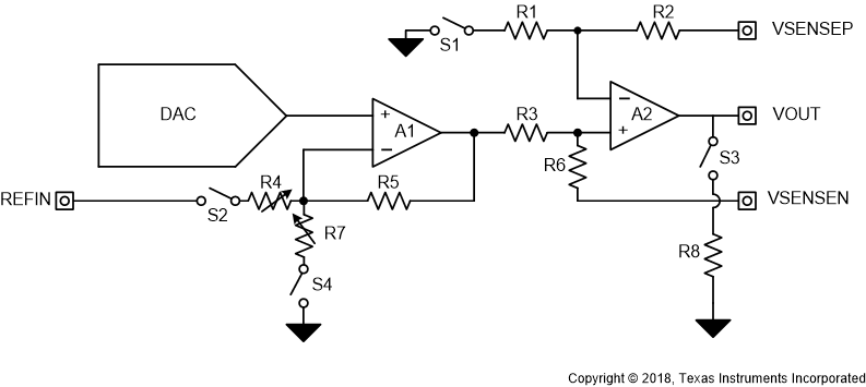
Figure 123 illustrates a simplified block diagram of the voltage output stages of the DAC8771.
 Figure 123. Simplified Block Diagram of Voltage Output Architecture
When designing for a shared voltage and current output terminal it is important to consider leakage paths that may corrupt the voltage or current output stages.
When the voltage output is active and the current output is inactive the IOUT pin becomes a high-impedance node and therefore does not significantly load the voltage output in a way that would degrade VOUT performance. When the voltage output is inactive and the current output is active switches S1, S2, and S4 all become open while switch S3 is controlled by the POC bit in the Reset Config Register. When the POC bit is set to a 0, the default value, switch S3 is closed when VOUT is disabled. This creates a leakage path with respect to the current output when the terminals are shared which will create a load dependent error. In order to reduce this error the POC bit can be set to a 1 which opens switch S3, effectively making the VOUT pin high-impedance and reducing the magnitude of leakage current.