SLASEJ4C April 2017 – February 2023 PGA460
PRODUCTION DATA
- 1 Features
- 2 Applications
- 3 Description
- 4 Revision History
- 5 Pin Configuration and Functions
-
6 Specifications
- 6.1 Absolute Maximum Ratings
- 6.2 ESD Ratings
- 6.3 Recommended Operating Conditions
- 6.4 Thermal Information
- 6.5 Internal Supply Regulators Characteristics
- 6.6 Transducer Driver Characteristics
- 6.7 Transducer Receiver Characteristics
- 6.8 Analog to Digital Converter Characteristics
- 6.9 Digital Signal Processing Characteristics
- 6.10 Temperature Sensor Characteristics
- 6.11 High-Voltage I/O Characteristics
- 6.12 Digital I/O Characteristics
- 6.13 EEPROM Characteristics
- 6.14 Timing Requirements
- 6.15 Switching Characteristics
- 6.16 Typical Characteristics
-
7 Detailed Description
- 7.1 Overview
- 7.2 Functional Block Diagram
- 7.3
Feature Description
- 7.3.1 Power-Supply Block
- 7.3.2 Burst Generation
- 7.3.3 Analog Front-End
- 7.3.4 Digital Signal Processing
- 7.3.5 System Diagnostics
- 7.3.6
Interface Description
- 7.3.6.1 Time-Command Interface
- 7.3.6.2
USART Interface
- 7.3.6.2.1 USART Asynchronous Mode
- 7.3.6.2.2 One-Wire UART Interface
- 7.3.6.2.3 Ultrasonic Object Detection Through UART Operations
- 7.3.6.3 In-System IO-Pin Interface Selection
- 7.3.7 Echo Data Dump
- 7.3.8 Low-Power Mode
- 7.3.9 Transducer Time and Temperature Decoupling
- 7.3.10 Memory CRC Calculation
- 7.3.11 Temperature Sensor and Temperature Data-Path
- 7.3.12 TEST Pin Functionality
- 7.4 Device Functional Modes
- 7.5 Programming
- 7.6 Register Maps
- 8 Application and Implementation
- 9 Device and Documentation Support
- 10Mechanical, Packaging, and Orderable Information
7.3.12 TEST Pin Functionality
The PGA460 TEST pin serves multiple purposes including:
- Allows the user to extract internal signals from the PGA460 device.
- Selects the output voltage of the digital pins which enables a 3.3-V MCU or a 5-V MCU to be connected to the device without using any external voltage translators. The RXD, TXD, SCLK, DECPL, and TEST pins are affected by this selection.
Internal signals on the TEST pin can be extracted by selecting a predefined signal through the internal test mux. The TEST_MUX register parameter is used to select this signal. Table 7-5 lists the possible PGA460 internal signals that are output at the TEST pin.
| TEST_MUX VALUE | SIGNAL NAME | TYPE | DESCRIPTION |
|---|---|---|---|
| 0x00 | Hi-Z (disabled) | Analog | The TEST pin is in the high impedance state |
| 0x01 | ASC Output | SAR ADC input after the ADC buffer | |
| 0x02 | Reserved | ||
| 0x03 | Reserved | ||
| 0x04 | 8MHz Clock | Digital | 8-MHz clock output from PGA460 |
| 0x05 | ADC Sample Clock | 1-µs ADC sample Clock | |
| 0x06 | Reserved | ||
| 0x07 | Reserved |
When used as an analog test-mux output, the TEST pin output voltage can change from 0 V to 1.8 V while the common mode voltage is set to 0.9 V.
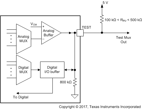
The digital voltage-level selection performed by the TEST pin is executed at device power up. On power-up, the device checks the level of the TEST pin. If the level is low, the digital output pins operate at 3.3 V. If the TEST pin is tied high (3.3 V or 5 V are both considered high state), the digital output pins operate at a 5 V. This condition is latched in the PGA460 device so that the test mux can further use the TEST pin as previously described. If the application requires that a 5-V digital output is used and a test mux output must be extracted from the PGA460 device, then a weak pullup resistor on the TEST pin can be connected as shown in #X2613.
 Figure 7-40 Test Pin Test Mux Output Application
As shown in #X2613, the resistor (RPU) is connected to a permanent power supply and a current path to ground is generated through the RPU resistor and the 800-kΩ internal resistance. This configuration is no problem for the system; however, it might cause a small quiescent-current increase in applications that require the use of the PGA460 low-power mode to preserve energy. In this case, the TEST pin can be connected to a GPIO pin on the external MCU that can output a logic low or high state on the TEST pin to select the voltage level at device start-up and later disable the GPIO output to preserve energy or reconfigure the GPIO as an input in case the MCU uses any of the PGA460 test output signals. The external pullup resistor is only required for CMOS 5-V UART communication and is not required for 3-V communication.