SLASEO5D March 2019 – September 2021 MSP430FR2672 , MSP430FR2673 , MSP430FR2675 , MSP430FR2676
PRODUCTION DATA
- 1 Features
- 2 Applications
- 3 Description
- 4 Functional Block Diagram
- 5 Revision History
- 6 Device Comparison
- 7 Terminal Configuration and Functions
-
8 Specifications
- 8.1 Absolute Maximum Ratings
- 8.2 ESD Ratings
- 8.3 Recommended Operating Conditions
- 8.4 Active Mode Supply Current Into VCC Excluding External Current
- 8.5 Active Mode Supply Current Per MHz
- 8.6 Low-Power Mode LPM0 Supply Currents Into VCC Excluding External Current
- 8.7 Low-Power Mode (LPM3, LPM4) Supply Currents (Into VCC) Excluding External Current
- 8.8 Low-Power Mode LPMx.5 Supply Currents (Into VCC) Excluding External Current
- 8.9 Typical Characteristics – Low-Power Mode Supply Currents
- 8.10 Current Consumption Per Module
- 8.11 Thermal Resistance Characteristics
- 8.12 Timing and Switching Characteristics
-
9 Detailed Description
- 9.1 Overview
- 9.2 CPU
- 9.3 Operating Modes
- 9.4 Interrupt Vector Addresses
- 9.5 Bootloader (BSL)
- 9.6 JTAG Standard Interface
- 9.7 Spy-Bi-Wire Interface (SBW)
- 9.8 FRAM
- 9.9 Memory Protection
- 9.10
Peripherals
- 9.10.1 Power-Management Module (PMM)
- 9.10.2 Clock System (CS) and Clock Distribution
- 9.10.3 General-Purpose Input/Output Port (I/O)
- 9.10.4 Watchdog Timer (WDT)
- 9.10.5 System (SYS) Module
- 9.10.6 Cyclic Redundancy Check (CRC)
- 9.10.7 Enhanced Universal Serial Communication Interface (eUSCI_A0, eUSCI_B0)
- 9.10.8 Timers (TA0, TA1, TA2, TA3 and TB0)
- 9.10.9 Hardware Multiplier (MPY)
- 9.10.10 Backup Memory (BAKMEM)
- 9.10.11 Real-Time Clock (RTC)
- 9.10.12 12-Bit Analog-to-Digital Converter (ADC)
- 9.10.13 eCOMP0
- 9.10.14 CapTIvate Technology
- 9.10.15 Embedded Emulation Module (EEM)
- 9.11
Input/Output Diagrams
- 9.11.1 Port P1 (P1.0 to P1.7) Input/Output With Schmitt Trigger
- 9.11.2 Port P2 (P2.0 to P2.7) Input/Output With Schmitt Trigger
- 9.11.3 Port P3 (P3.0 to P3.7) Input/Output With Schmitt Trigger
- 9.11.4 Port P4 (P4.0 to P4.7) Input/Output With Schmitt Trigger
- 9.11.5 Port P5 (P5.0 to P5.7) Input/Output With Schmitt Trigger
- 9.11.6 Port P6 (P6.0 to P6.2) Input/Output With Schmitt Trigger
- 9.12 Device Descriptors
- 9.13 Memory
- 9.14 Identification
- 10Applications, Implementation, and Layout
- 11Device and Documentation Support
- 12Mechanical, Packaging, and Orderable Information
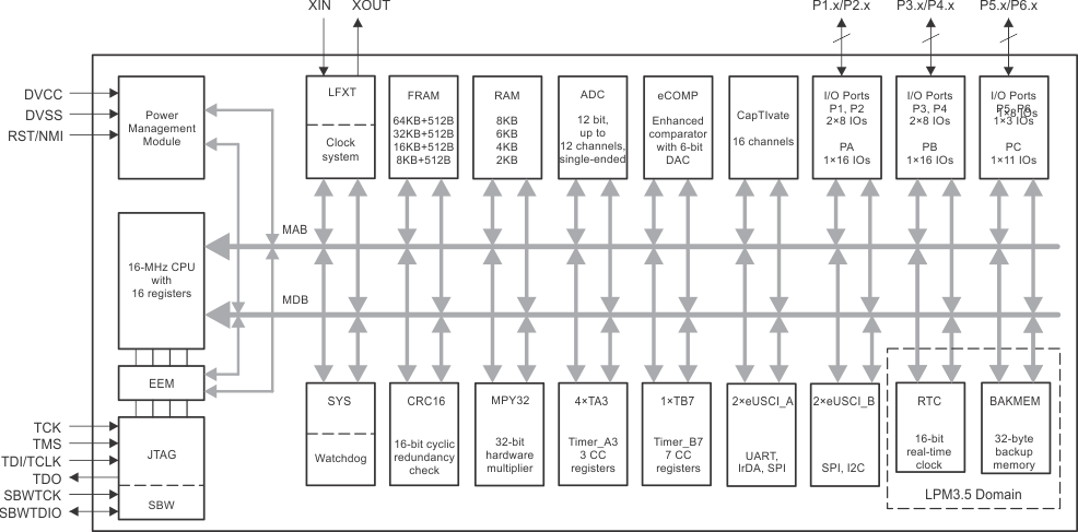
4 Functional Block Diagram
Figure 4-1 shows the functional block diagram.
 Figure 4-1 Functional Block Diagram
- The MCU has one main power pair of DVCC and DVSS that supplies digital and analog modules. Recommended bypass and decoupling capacitors are 4.7 µF to 10 µF and 0.1 µF, respectively, with ±5% accuracy.
- VREG is the decoupling capacitor of the CapTIvate regulator. The recommended value for the required decoupling capacitor is 1 µF, with a maximum ESR of ≤200 mΩ.
- All GPIOs feature the pin interrupt function and can wake the MCU from all LPMs.
- In LPM3 or LPM4 mode, the CapTIvate module can be functional while the rest of the peripherals are off.