SLASEQ4A October   2018  – December 2018 DAC43608 , DAC53608

PRODUCTION DATA.  

  1. Features
  2. Applications
  3. Description
    1.     Device Images
      1.      Simplified Block Diagram
      2.      Programmable Window Comparator
  4. Revision History
  5. Device Comparison Table
  6. Pin Configurations and Functions
    1.     Pin Functions
  7. Specifications
    1. 7.1  Absolute Maximum Ratings
    2. 7.2  ESD Ratings
    3. 7.3  Recommended Operating Conditions
    4. 7.4  Thermal Information
    5. 7.5  Electrical Characteristics
    6. 7.6  Timing Requirements: I2CTM Standard Mode
    7. 7.7  Timing Requirements: I2CTM Fast Mode
    8. 7.8  Timing Requirements: I2CTM Fast+ Mode
    9. 7.9  Timing Requirements: Logic
    10. 7.10 Typical Characteristics: 1.8 V
    11. 7.11 Typical Characteristics: 5.5 V
    12. 7.12 Typical Characteristics
    13. 7.13 Typical Characteristics
  8. Detailed Description
    1. 8.1 Overview
    2. 8.2 Functional Block Diagram
    3. 8.3 Feature Description
      1. 8.3.1 Digital-to-Analog Converter (DAC) Architecture
        1. 8.3.1.1 DAC Transfer Function
        2. 8.3.1.2 DAC Register Update and LDAC Functionality
        3. 8.3.1.3 CLR Functionality
        4. 8.3.1.4 Output Amplifier
      2. 8.3.2 Reference
      3. 8.3.3 Power-on-Reset (POR)
      4. 8.3.4 Software Reset
    4. 8.4 Device Functional Modes
      1. 8.4.1 Power-Down Mode
    5. 8.5 Programming
      1. 8.5.1 F/S Mode Protocol
      2. 8.5.2 DACx3608 I2CTM Update Sequence
      3. 8.5.3 DACx3608 Address Byte
      4. 8.5.4 DACx3608 Command Byte
      5. 8.5.5 DACx3608 Data Byte (MSDB and LSDB)
      6. 8.5.6 DACx3608 I2CTM Read Sequence
    6. 8.6 Register Map
      1. 8.6.1 DEVICE_CONFIG Register (offset = 01h) [reset = 00FFh]
        1. Table 10. DEVICE_CONFIG Register Field Descriptions
      2. 8.6.2 STATUS/TRIGGER Register (offset = 02h) [reset = 0300h for DAC53608, reset = 0500h for DAC43608]
        1. Table 11. STATUS/TRIGGER Register Field Descriptions
      3. 8.6.3 BRDCAST Register (offset = 03h) [reset = 0000h]
        1. Table 12. BRDCAST Register Field Descriptions
      4. 8.6.4 DACn_DATA Register (offset = 08h to 0Fh) [reset = 0000h]
        1. Table 13. DACn_DATA Register Field Descriptions
  9. Application and Implementation
    1. 9.1 Application Information
    2. 9.2 Typical Applications
      1. 9.2.1 Programmable LED Biasing
        1. 9.2.1.1 Design Requirements
        2. 9.2.1.2 Detailed Design Procedure
        3. 9.2.1.3 Application Curve
      2. 9.2.2 Programmable Window Comparator
        1. 9.2.2.1 Design Requirements
        2. 9.2.2.2 Detailed Design Procedure
        3. 9.2.2.3 Application Curve
  10. 10Power Supply Recommendations
  11. 11Layout
    1. 11.1 Layout Guidelines
    2. 11.2 Layout Example
  12. 12Device and Documentation Support
    1. 12.1 Documentation Support
      1. 12.1.1 Related Documentation
    2. 12.2 Related Links
    3. 12.3 Receiving Notification of Documentation Updates
    4. 12.4 Community Resources
    5. 12.5 Trademarks
    6. 12.6 Electrostatic Discharge Caution
    7. 12.7 Glossary
  13. 13Mechanical, Packaging, and Orderable Information

Typical Characteristics: 5.5 V

at TA = 25°C, VDD = 5.5 V, reference = 5.5 V, and DAC outputs unloaded (unless otherwise noted)
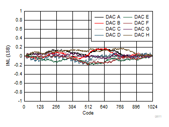
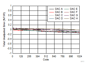
DAC53608 DAC43608 D011.gif
Figure 12. Integral Linearity Error vs Digital Input Code
DAC53608 DAC43608 D013.gif
Figure 14. Total Unadjusted Error vs Digital Input Code
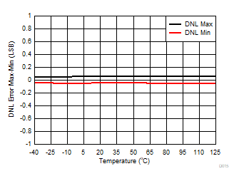
DAC53608 DAC43608 D015.gif
Figure 16. Differential Linearity Error vs Temperature
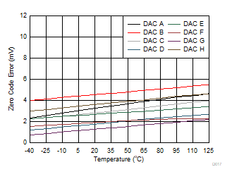
DAC53608 DAC43608 D017.gif
Figure 18. Zero Code Error vs Temperature
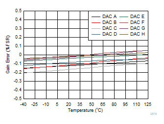
DAC53608 DAC43608 D019.gif
Figure 20. Gain Error vs Temperature
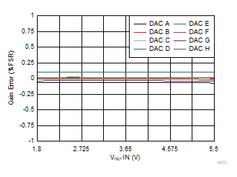
DAC53608 DAC43608 D033.gif
Figure 22. Gain Error vs Reference Voltage
DAC53608 DAC43608 D035.gif
at VDD = 1.8 V and reference = 1.8 V
Figure 24. Supply Current vs Digital Input Code
DAC53608 DAC43608 D037.gif
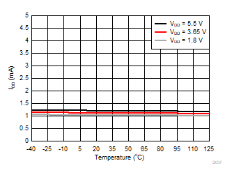
DAC code at mid-scale
Figure 26. Supply Current vs Temperature
DAC53608 DAC43608 D039.gif
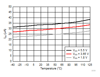
Figure 28. Power Down Current vs Temperature
DAC53608 DAC43608 D042.gif
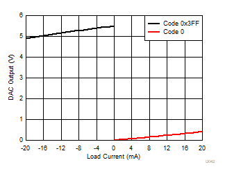
at VDD = 5.5 V and reference = 5.5 V
Figure 30. Source and Sink Capability
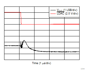
DAC53608 DAC43608 D044.gif
DAC code transition from mid-scale to mid-scale – 1 LSB, DAC output loaded with 5 kΩ//200 pF
Figure 32. Glitch Impulse, Falling Edge, 1 LSB Step
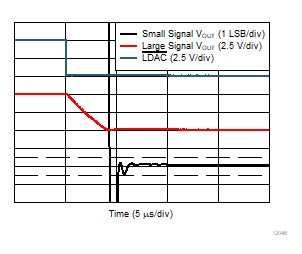
DAC53608 DAC43608 D046.gif
DAC code transition from 922d to 102d, typical channel shown, DAC output loaded with 5 kΩ//200 pF
Figure 34. Full-Scale Settling Time, Falling Edge
DAC53608 DAC43608 D048.gif
DAC output loaded with 5 kΩ//200 pF
Figure 36. Power-off Glitch
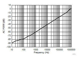
DAC53608 DAC43608 D050.gif
DAC code at full-scale and output loaded with 5 kΩ//200 pF, VDD = 5.25 V + 0.2 VPP and VREFIN = 4.5 V
Figure 38. DAC Output AC PSRR vs Frequency
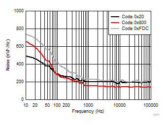
DAC53608 DAC43608 D051.gif
Figure 40. DAC Output Noise Spectral Density
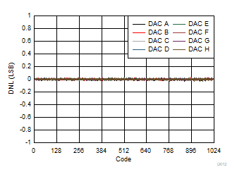
DAC53608 DAC43608 D012.gif
Figure 13. Differential Linearity Error vs Digital Input Code
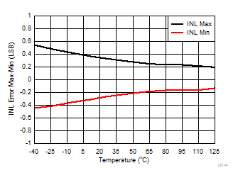
DAC53608 DAC43608 D014.gif
Figure 15. Integral Linearity Error vs Temperature
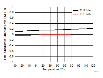
DAC53608 DAC43608 D016.gif
Figure 17. Total Unadjusted Error vs Temperature
DAC53608 DAC43608 D018.gif
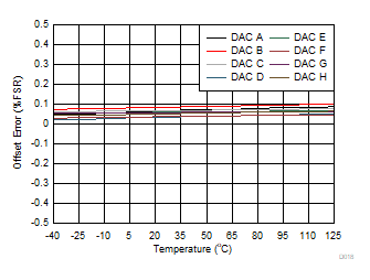
Figure 19. Offset Error vs Temperature
DAC53608 DAC43608 D020.gif
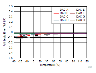
Figure 21. Full Scale Error vs Temperature
DAC53608 DAC43608 D034.gif
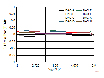
Figure 23. Full Scale Error vs Reference Voltage
DAC53608 DAC43608 D036.gif
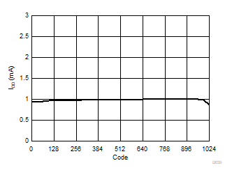
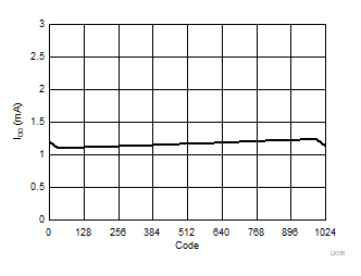
at VDD = 5.5 V and reference = 5.5 V
Figure 25. Supply Current vs Digital Input Code
DAC53608 DAC43608 D038.gif
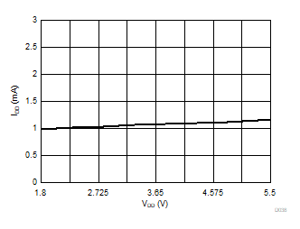
DAC code at mid-scale and reference tied to VDD
Figure 27. Supply Current vs Supply Voltage
DAC53608 DAC43608 D041.gif
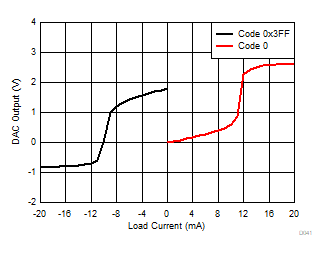
at VDD = 1.8 V and reference = 1.8 V
Figure 29. Source and Sink Capability
DAC53608 DAC43608 D043.gif
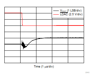
DAC code transition from mid-scale – 1 to mid-scale, DAC output loaded with 5 kΩ//200 pF
Figure 31. Glitch Impulse, Rising Edge, 1 LSB Step
DAC53608 DAC43608 D045.gif
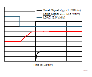
DAC code transition from 102d to 922d, typical channel shown, DAC output loaded with 5 kΩ//200 pF
Figure 33. Full-Scale Settling Time, Rising Edge
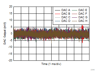
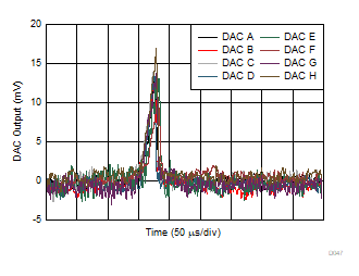
DAC53608 DAC43608 D047.gif
DAC output loaded with 5 kΩ//200 pF
Figure 35. Power-on Glitch
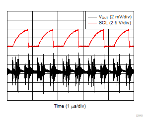
DAC53608 DAC43608 D049.gif
DAC code at mid-scale and reference tied to VDD and output loaded with 5 kΩ//200 pF
Figure 37. Clock Feedthrough with SCL = 1 MHz
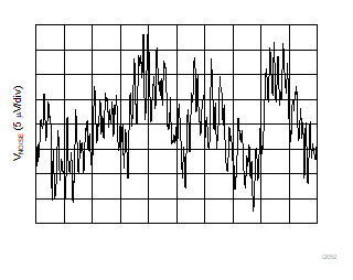
DAC53608 DAC43608 D052.gif
DAC code at mid-scale
Figure 39. DAC Output Noise 0.1 Hz to 10 Hz