SLASF08A December 2021 – May 2024 DAC43508 , DAC53508 , DAC63508
PRODUCTION DATA
- 1
- 1 Features
- 2 Applications
- 3 Description
- 4 Pin Configurations and Functions
-
5 Specifications
- 5.1 Absolute Maximum Ratings
- 5.2 ESD Ratings
- 5.3 Recommended Operating Conditions
- 5.4 Thermal Information
- 5.5 Electrical Characteristics
- 5.6 Timing Requirements: SPI
- 5.7 Timing Requirements: Logic
- 5.8 Timing Diagrams
- 5.9 Typical Characteristics: Static Performance
- 5.10 Typical Characteristics: Dynamic Performance
- 5.11 Typical Characteristics: General
- 6 Detailed Description
- 7 Register Map
- 8 Application and Implementation
- 9 Device and Documentation Support
- 10Revision History
- 11Mechanical, Packaging, and Orderable Information
6.3.3 Power-On Reset (POR)
The DACx3508 family of devices includes a power-on reset (POR) function that controls the output voltage at power up. After the VDD supply has been established, a POR event is issued. The POR causes all registers to initialize to default values, and communication with the device is valid only after a 5-ms delay, when VDD reaches DAC operating range. The default value for the DAC data registers is zero code. The DAC output remains at the power-up voltage until a valid command is written to a channel.
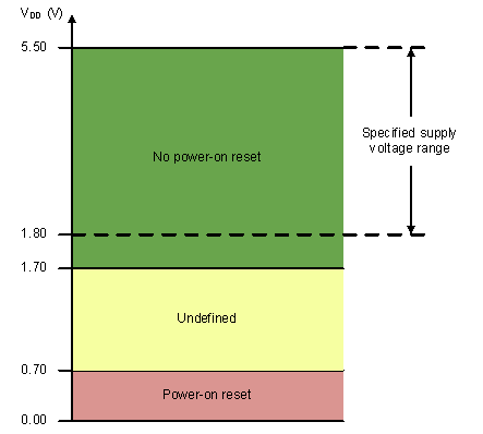
When the device powers up, a POR circuit sets the device to the default mode. The POR circuit requires specific VDD levels, as indicated in Figure 6-2, to discharge the internal capacitors and reset the device on power up. To trigger a POR, VDD must be less than 0.7 V for at least 1 ms. When VDD drops to less than 1.7 V but remains greater than 0.7 V (shown as the undefined region), the device does not reset successfully under all specified temperature and power-supply conditions. In this case, initiate a POR. When VDD remains greater than 1.7 V, a POR does not occur.
 Figure 6-2 Threshold Levels for VDD POR Circuit