SLAU298A November 2009 – May 2021
- Trademarks
- 1ADS8555EVM-PDK Overview
- 2EVM Analog Interface
- 3Digital Interface
- 4Power Supplies
- 5Installing the ADS8555EVM Software
-
6ADS8555EVM Operation
- 6.1 Connecting the Hardware and Running the GUI
- 6.2 Jumper Settings for the ADS8555EVM
- 6.3 Modifying Hardware and Using Software to Evaluate Other Devices in the Family
- 6.4 EVM GUI Global Settings for ADC Control and Registers
- 6.5 Time Domain Display
- 6.6 Frequency Domain Display
- 6.7 Histogram Display
- 7Bill of Materials, Layout, and Schematics
- 8Revision History
2.2 ADC Amplifier Drive
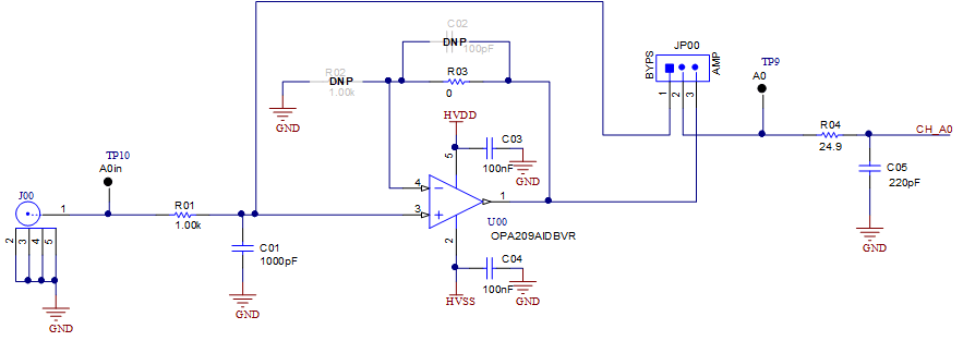
Figure 2-2 shows the op amp configuration for each ADC drive input. The default configuration is a noninverting buffer configuration. The gain of this circuit can be adjusted by changing R03 and R02 as needed. C02 can be used to limit the amplifier bandwidth or compensate the amplifier. R01 and C01 can also be used to create a low-pass filter. Jumper JP00 can be used to completely bypass the amplifier. This diagram only shows one channel, but this circuit is repeated six times. For other channels, see Figure 7-2.
 Figure 2-2 Amplifier Drive Circuit