SLAU320AJ July   2010  – May 2021


  1.   Trademarks
  2. 1Introduction
    1. 1.1 About This Document
    2. 1.2 Organization of This Document
  3. 2Programming Using the JTAG Interface
    1. 2.1 Introduction
      1. 2.1.1 MSP430 JTAG Restrictions (Noncompliance With IEEE Std 1149.1)
      2. 2.1.2 TAP Controller State Machine
    2. 2.2 Interface and Instructions
      1. 2.2.1 JTAG Interface Signals
        1. 2.2.1.1 Pros and Cons of 2-Wire Spy-Bi-Wire and 4-Wire JTAG
        2. 2.2.1.2 4-Wire JTAG Interface
        3. 2.2.1.3 2-Wire Spy-Bi-Wire (SBW) JTAG Interface
      2. 2.2.2 JTAG Access Macros
        1. 2.2.2.1 Macros for 4-Wire JTAG Interface
          1. 2.2.2.1.1 IR_SHIFT (8-Bit Instruction)
          2. 2.2.2.1.2 DR_SHIFT16 (16-Bit Data)
          3. 2.2.2.1.3 DR_SHIFT20 (20-Bit Address) (Applies Only to MSP430X Devices)
          4. 2.2.2.1.4 MsDelay (Time)
          5. 2.2.2.1.5 SetTCLK
          6. 2.2.2.1.6 ClrTCLK
        2. 2.2.2.2 Macros for Spy-Bi-Wire (SBW) Interface
      3. 2.2.3 Spy-Bi-Wire (SBW) Timing and Control
        1. 2.2.3.1 Basic Timing
        2. 2.2.3.2 TMS Slot
          1. 2.2.3.2.1 TMSH Macro
          2. 2.2.3.2.2 TMSL Macro
          3. 2.2.3.2.3 TMSLDH Macro
        3. 2.2.3.3 TDI Slot
          1. 2.2.3.3.1 TDIH Macro
          2. 2.2.3.3.2 TDIL Macro
        4. 2.2.3.4 TDO Slot
          1. 2.2.3.4.1 TDO_RD Macro
          2. 2.2.3.4.2 TDOsbw Macro (No Read)
        5. 2.2.3.5 TCLK Handling in Spy-Bi-Wire (SBW) Mode
          1. 2.2.3.5.1 SetTCLK and ClrTCLK
          2. 2.2.3.5.2 TCLK Strobes
      4. 2.2.4 JTAG Communication Instructions
        1. 2.2.4.1 Controlling the Memory Address Bus (MAB)
          1. 2.2.4.1.1 IR_ADDR_16BIT
          2. 2.2.4.1.2 IR_ADDR_CAPTURE
        2. 2.2.4.2 Controlling the Memory Data Bus (MDB)
          1. 2.2.4.2.1 IR_DATA_TO_ADDR
          2. 2.2.4.2.2 IR_DATA_16BIT
          3. 2.2.4.2.3 IR_DATA_QUICK
          4. 2.2.4.2.4 IR_BYPASS
        3. 2.2.4.3 Controlling the CPU
          1. 2.2.4.3.1 IR_CNTRL_SIG_16BIT
          2. 2.2.4.3.2 IR_CNTRL_SIG_CAPTURE
          3. 2.2.4.3.3 IR_CNTRL_SIG_RELEASE
        4. 2.2.4.4 Memory Verification by Pseudo Signature Analysis (PSA)
          1. 2.2.4.4.1 IR_DATA_PSA
          2. 2.2.4.4.2 IR_SHIFT_OUT_PSA
        5. 2.2.4.5 JTAG Access Security Fuse Programming
          1. 2.2.4.5.1 IR_PREPARE_BLOW
          2. 2.2.4.5.2 IR_EX_BLOW
    3. 2.3 Memory Programming Control Sequences
      1. 2.3.1 Start-Up
        1. 2.3.1.1 Enable JTAG Access
        2. 2.3.1.2 Fuse Check and Reset of the JTAG State Machine (TAP Controller)
      2. 2.3.2 General Device (CPU) Control Functions
        1. 2.3.2.1 Function Reference for 1xx, 2xx, 4xx Families
          1. 2.3.2.1.1 Taking the CPU Under JTAG Control
          2. 2.3.2.1.2 Set CPU to Instruction-Fetch
          3. 2.3.2.1.3 Setting the Target CPU Program Counter (PC)
          4. 2.3.2.1.4 Controlled Stop or Start of the Target CPU
          5. 2.3.2.1.5 Resetting the CPU While Under JTAG Control
          6. 2.3.2.1.6 Release Device From JTAG Control
        2. 2.3.2.2 Function Reference for 5xx and 6xx Families
          1. 2.3.2.2.1 Taking the CPU Under JTAG Control
          2. 2.3.2.2.2 Setting the Target CPU Program Counter (PC)
          3. 2.3.2.2.3 Resetting the CPU While Under JTAG Control
          4. 2.3.2.2.4 Release Device From JTAG Control
          5. 2.3.2.2.5 74
      3. 2.3.3 Accessing Non-Flash Memory Locations With JTAG
        1. 2.3.3.1 Read Access
        2. 2.3.3.2 Write Access
        3. 2.3.3.3 Quick Access of Memory Arrays
          1. 2.3.3.3.1 Flow for Quick Read (All Memory Locations)
          2. 2.3.3.3.2 Flow for Quick Write
      4. 2.3.4 Programming the Flash Memory (Using the Onboard Flash Controller)
        1. 2.3.4.1 Function Reference for 1xx, 2xx, 4xx Families
        2. 2.3.4.2 Function Reference for 5xx and 6xx Families
      5. 2.3.5 Erasing the Flash Memory (Using the Onboard Flash Controller)
        1. 2.3.5.1 Function Reference for 1xx, 2xx, 4xx Families
          1. 2.3.5.1.1 Flow to Erase a Flash Memory Segment
          2. 2.3.5.1.2 Flow to Erase the Entire Flash Address Space (Mass Erase)
        2. 2.3.5.2 Function Reference for 5xx and 6xx Families
      6. 2.3.6 Reading From Flash Memory
      7. 2.3.7 Verifying the Target Memory
      8. 2.3.8 FRAM Memory Technology
        1. 2.3.8.1 Writing and Reading FRAM
        2. 2.3.8.2 Erasing FRAM
    4. 2.4 JTAG Access Protection
      1. 2.4.1 Burning the JTAG Fuse - Function Reference for 1xx, 2xx, 4xx Families
        1. 2.4.1.1 Standard 4-Wire JTAG
          1. 2.4.1.1.1 Fuse-Programming Voltage on TDI Pin (Dedicated JTAG Pin Devices Only)
          2. 2.4.1.1.2 Fuse-Programming Voltage On TEST Pin
        2. 2.4.1.2 Fuse-Programming Voltage Using SBW
      2. 2.4.2 Programming the JTAG Lock Key - Function Reference for 5xx, 6xx, and FRxx Families
        1. 2.4.2.1 Flash Memory Devices
        2. 2.4.2.2 FRAM Memory Devices
      3. 2.4.3 Testing for a Successfully Protected Device
      4. 2.4.4 Unlocking an FRAM Device in Protected and Secured Modes
        1. 2.4.4.1 FR5xx and FR6xx Devices
        2. 2.4.4.2 FR4xx and FR2xx Devices
      5. 2.4.5 Memory Protection Unit Handling
      6. 2.4.6 Intellectual Property Encapsulation (IPE)
      7. 2.4.7 FRAM Write Protection
    5. 2.5 JTAG Function Prototypes
      1. 2.5.1 Low-Level JTAG Functions
      2. 2.5.2 High-Level JTAG Routines
    6. 2.6 JTAG Features Across Device Families
    7. 2.7 References
  4. 3JTAG Programming Hardware and Software Implementation
    1. 3.1 Implementation History
    2. 3.2 Implementation Overview
    3. 3.3 Software Operation
    4. 3.4 Software Structure
      1. 3.4.1 Programmer Firmware
      2. 3.4.2 Target Code
        1. 3.4.2.1 Target Code Download for Replicator430, Replicator430X, and Replicator430Xv2
        2. 3.4.2.2 Target Code Download for Replicator430FR (FRAM)
    5. 3.5 Hardware Setup
      1. 3.5.1 Host Controller
      2. 3.5.2 Target Connection
      3. 3.5.3 Host Controller or Programmer Power Supply
      4. 3.5.4 Third-Party Support
  5. 4Errata and Revision Information
    1. 4.1 Known Issues
    2. 4.2 Revisions and Errata From Previous Documents
  6. 5Revision History
Taking the CPU Under JTAG Control

Reference function: GetDevice_430Xv2

For the 5xx and 6xx families, the CPU is taken under JTAG control by setting bit 10 (TCE1) of the JTAG control signal register to 1. While the flow to take the target device under JTAG control is identical to the flow described in Section 2.3.2.1.1, additional actions must be taken to completely take over control of the target CPU; for example, it is not recommended to take over control without performing a CPU reset by setting the POR signal in the JTAG Control Signal Register. Also, care must be taken that the CPU is in the Full-Emulation-State (equivalent to the Instruction-Fetch state for MSP430 and MSP430X architectures) by setting the CPUSUSP signal and providing a number of TCLK until the CPU prefetch pipes are cleared. Figure 2-15 shows the full sequence required to get the CPU in the Full-Emulation-State.
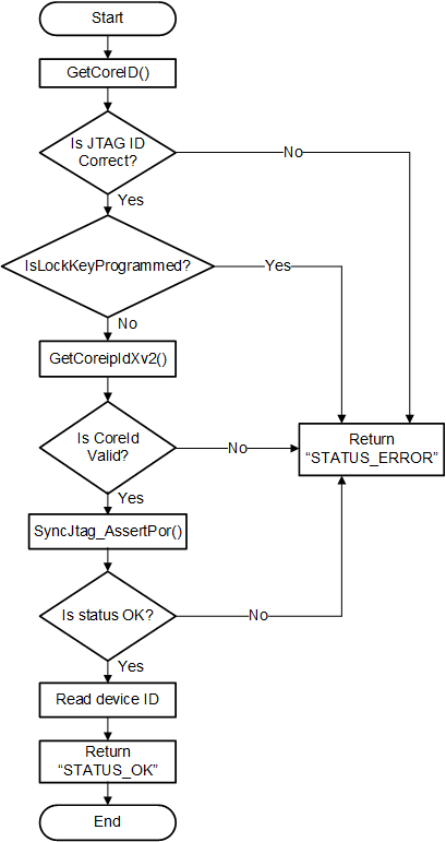
GUID-AD0BB602-1625-4FD5-B6A4-426284D965D8-low.gif Figure 2-15 Taking the CPU Under JTAG Control

Reference function: GetCoreID

Figure 2-16 shows the JTAG-entry sequence for MSP430Xv2 devices. If no valid JTAG-ID is returned by the first entry sequence approach, a second one that uses a "magic pattern" is executed. The differences between these two entry approaches is: the second approach holds the device in reset and shifts in a "magic pattern" (0xA55A) by using the JTAG mailbox. The magic pattern is read by the BootCode, and the device is sent into LPM4. If the device is in LPM4, no user code is executed. The magic pattern mode forces a reset of the device.

In the special case that the device is in LPMx.5 (low-power mode where JTAG is unpowered and the JTAG pins are locked by the ioLock), another mechanism is needed to take the device under JTAG control. Only the TEST and the REST pin are not pulled down by the ioLock. That means that these pins must be used to get control over the device. Compared to the normal SBW communication, which uses TDI/TDO and TMS pins in the replicator implementation, TEST and RST are used for SBW communication to disable the ioLock.
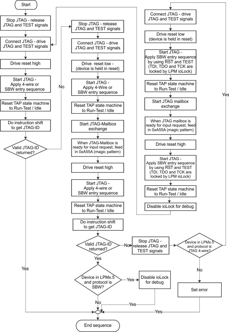
GUID-FFED8313-2748-41AD-BDE5-5E3830119F88-low.gif Figure 2-16 JTAG Entry Sequence for 430Xv2 Devices
  • Reference function: GetCoreipIdXv2()
    IR_Shift(IR_COREIP_ID)
    CoreId = DR_Shift16(0)
    CoreId = 0 ? Yes
    No
    IR_Shift(IR_DEVICE_ID)
    DeviceIdPointer = DR_Shift20(0)
  • Reference function: SyncJtag_AssertPor()
    IR_SHIFT("IR_CNTRL_SIG_16BIT")
    DR_SHIFT16(0x1501)
    IR_SHIFT("IR_CNTRL_SIG_CAPTURE")
    DR_SHIFT16(0x0000) No
    Bit 9 of TDOword = 1?
    Yes
    CPU is under JTAG control - always apply Power on Reset (POR) afterwards.