SLAU320AJ July 2010 – May 2021
- Trademarks
- 1Introduction
-
2Programming Using the JTAG Interface
- 2.1 Introduction
- 2.2
Interface and Instructions
- 2.2.1 JTAG Interface Signals
- 2.2.2 JTAG Access Macros
- 2.2.3 Spy-Bi-Wire (SBW) Timing and Control
- 2.2.4 JTAG Communication Instructions
- 2.3
Memory Programming Control Sequences
- 2.3.1 Start-Up
- 2.3.2 General Device (CPU) Control Functions
- 2.3.3 Accessing Non-Flash Memory Locations With JTAG
- 2.3.4 Programming the Flash Memory (Using the Onboard Flash Controller)
- 2.3.5 Erasing the Flash Memory (Using the Onboard Flash Controller)
- 2.3.6 Reading From Flash Memory
- 2.3.7 Verifying the Target Memory
- 2.3.8 FRAM Memory Technology
- 2.4
JTAG Access Protection
- 2.4.1 Burning the JTAG Fuse - Function Reference for 1xx, 2xx, 4xx Families
- 2.4.2 Programming the JTAG Lock Key - Function Reference for 5xx, 6xx, and FRxx Families
- 2.4.3 Testing for a Successfully Protected Device
- 2.4.4 Unlocking an FRAM Device in Protected and Secured Modes
- 2.4.5 Memory Protection Unit Handling
- 2.4.6 Intellectual Property Encapsulation (IPE)
- 2.4.7 FRAM Write Protection
- 2.5 JTAG Function Prototypes
- 2.6 JTAG Features Across Device Families
- 2.7 References
- 3JTAG Programming Hardware and Software Implementation
- 4Errata and Revision Information
- 5Revision History
2.3.4.2 Function Reference for 5xx and 6xx Families
Because the 5xx and 6xx devices have a dedicated timing generator available on chip, flash access is significantly easier compared to the other MSP430 families. There is no need for the user to ensure a certain erase or program frequency on the TCLK signal. All timings that are required for memory erase and write access are generated automatically.
The basis for the following description is that the flash memory access operation can be initiated from within RAM, as described in the relevant MSP430F5xx and MSP430F6xx Family User's Guide chapters. This document describes how to load an appropriate code in the target device RAM and how to control the correct execution of the code using the JTAG interface. Controlling the execution of the target code can be done by releasing the device from JTAG control. Releasing the device from JTAG control makes the CPU execute the program code in free running mode. After the desired operation is finished, the device must be taken under JTAG control again.
This method has advantages and disadvantages. Having a free-running device can increase flash programming speed to its upper limit; it requires a polling mechanism through JTAG to retrieve the current target device state. On the other hand, such a polling mechanism is not suitable for systems in which more than one target device is accessed in parallel. As all targets would not run at exactly the same frequency, keeping them under JTAG control would be the recommended approach for a parallel access system. This is not implemented in the REP430 firmware.
Exchanging information between the target devices' CPU and JTAG (for example, for device state polling purposes) uses a new feature of the 5xx JTAG implementation: The JTAG mailbox system. The idea behind the JTAG mailbox system is to have a direct interface to the CPU during debugging, programming, and test that is identical for all devices in this family and that uses few or no user application resources (refer to the MSP430F5xx and MSP430F6xx Family User's Guide System Resets, Interrupts and Operating Modes, System Control Module (SYS) chapter).
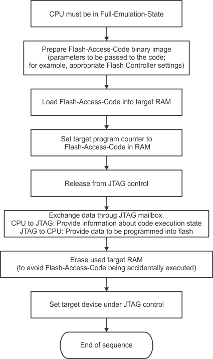
Figure 2-17 shows the general flow required to perform flash memory operations on 5xx and 6xx devices through the JTAG interface. The term Flash-Access-Code stands for an appropriate executable MSP430 code that can be used to perform the flash access operation. The following sections use the term Flash-Write-Code for code that is used to program the flash memory and Flash-Erase-Code for code that is used to erase the flash memory.
 Figure 2-17 Accessing Flash Memory
Reference function: WriteFLASH_430Xv2
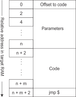
This section describes one method to program the flash memory subsequently with 16-bit word data by executing an appropriate Flash-Write-Code in RAM and providing the data to the CPU through the JTAG mailbox system. The provided source code example includes a Flash-Write-Code example that has the capability to be parameterized in binary state. Figure 2-18 shows a generic map of the binary image of the flash access codes provided with this document.
 Figure 2-18 Flash Access Code Binary Image Map
- The code is position independent.
- The first address holds an offset value relative to the actual program code start address. The current address plus the offset value results in the value that must be assigned to the Program Counter before starting execution of the code.
- Space for code specific parameters.
- Actual program code.
- Endless loop at the end.
The Flash-Write-Code in particular takes the following parameters:
- StartAddr: First address in target memory to be written to
- Length: Number of 16-bit words to be written
- FCTL3: The value to be written into FCTL3 of the flash controller module (basically to define whether LOCKA should be set or not)
When executing the Flash-Write-Code, the data to be programmed into the target flash memory must be provided through the JTAG mailbox system. The following sequence shows how this is established.
- Released from JTAG control
Target device is released from JTAG control (free running) IR_SHIFT("IR_JB_EXCHANGE")Yes DR_SHIFT16(0x0000)No Bit 0 of TDOword = 1 ? Yes DR_SHIFT16(0x0001): Send input request to JTAG mailboxDR_SHIFT16("Data"): Shift 16 bit word into JTAG mailboxWrite Another Flash Address? No Get target device in Full-Emulation-State