SLAU723A October 2017 – October 2018 MSP432E401Y , MSP432E411Y
- 1
- 7
- 65
- 132
-
167
- 168
-
215
- 216
- 217
- 218
- 219
- 220
- 221
- 222
- 223
- 224
- 225
- 226
- 227
- 228
- 229
- 230
- 231
- 232
- 233
- 234
- 235
- 236
- 237
- 238
- 239
- 240
- 241
- 242
- 243
- 244
- 245
- 246
- 247
- 248
- 249
- 250
- 251
- 252
- 253
- 254
- 255
- 256
- 257
- 258
- 259
- 260
- 261
- 262
- 263
- 264
- 265
- 266
- 267
- 268
- 269
- 270
- 271
- 272
- 273
- 274
- 275
- 276
- 277
- 278
- 279
- 280
- 281
- 282
- 283
- 284
- 285
- 286
- 287
- 288
- 289
- 290
- 291
- 292
- 293
- 294
- 295
- 296
- 297
- 298
- 299
- 300
- 301
- 302
- 303
- 304
- 305
- 306
- 307
- 308
- 309
- 310
- 311
- 312
- 313
- 314
- 315
- 316
- 317
- 318
- 319
- 320
- 321
- 322
- 323
- 324
- 325
- 326
- 327
- 328
- 329
- 330
- 331
- 332
- 333
- 334
- 335
- 336
- 337
- 338
- 339
- 340
- 341
- 342
- 343
- 344
- 345
- 346
- 347
- 348
- 349
- 350
- 351
- 352
- 353
- 354
- 355
- 356
- 357
- 358
- 359
- 360
- 361
- 362
- 363
- 364
- 365
- 366
- 367
- 368
- 369
- 370
- 371
- 372
- 373
- 374
- 375
- 376
- 377
- 378
- 379
- 380
- 381
- 382
- 383
- 384
- 385
- 386
- 387
- 388
- 389
- 390
- 391
- 392
- 393
- 394
- 395
- 396
- 397
- 398
- 399
- 400
- 401
- 402
- 403
- 404
- 405
- 406
- 408
- 415
- 482
- 564
- 643
- 715
- 791
- 841
- 855
- 870
-
917
- 918
- 919
- 920
- 1002
- 1017
-
1021
- 1022
- 1023
- 1024
- 1025
- 1026
- 1027
- 1028
- 1029
- 1030
- 1031
- 1032
- 1033
- 1034
- 1035
- 1036
- 1037
- 1038
- 1039
- 1040
- 1041
- 1042
- 1043
- 1044
- 1045
- 1046
- 1047
- 1048
- 1049
- 1050
- 1051
- 1052
- 1053
- 1054
- 1055
- 1056
- 1057
- 1058
- 1059
- 1060
- 1061
- 1062
- 1063
- 1064
- 1065
- 1066
- 1067
- 1068
- 1069
- 1070
- 1071
- 1072
- 1073
- 1074
- 1075
- 1076
- 1077
- 1078
- 1079
- 1080
- 1081
- 1082
- 1083
- 1084
- 1085
- 1086
- 1087
- 1088
- 1089
- 1090
- 1091
- 1092
- 1093
- 1094
- 1095
- 1125
- 1189
- 1251
- 1304
- 1365
- 1431
- 1478
- 1503
- 1552
- 1569
- 1618
-
1669
- 1670
- 1671
- 1672
- 1723
-
1726
- 1727
- 1728
- 1729
- 1730
- 1731
- 1732
- 1733
- 1734
- 1735
- 1736
- 1737
- 1738
- 1739
- 1740
- 1741
- 1742
- 1743
- 1744
- 1745
- 1746
- 1747
- 1748
- 1749
- 1750
- 1751
- 1752
- 1753
- 1754
- 1755
- 1756
- 1757
- 1758
- 1759
- 1760
- 1761
- 1762
- 1763
- 1764
- 1765
- 1766
- 1767
- 1768
- 1769
- 1770
- 1771
- 1772
- 1773
- 1774
- 1775
- 1776
- 1777
- 1778
- 1779
- 1780
- 1781
- 1782
- 1783
- 1784
- 1785
- 1786
- 1787
- 1788
- 1789
- 1790
- 1791
- 1792
- 1793
- 1794
- 1795
- 1796
- 1797
- 1798
- 1799
- 1800
- 1801
- 1802
- 1803
- 1804
- 1805
- 1806
- 1833
18.3.3.5 PWM Mode
The GPTM supports a simple PWM generation mode. In PWM mode, the timer is configured as a 24-bit down counter with a start value (and thus period) defined by the GPTMTnILR and GPTMTnPR registers. In this mode, the PWM frequency and period are synchronous events and therefore guaranteed to be glitch-free. PWM mode is enabled with the GPTMTnMR register by setting the TnAMS bit to 0x1, the TnCMR bit to 0x0, and the TnMR field to 0x2. Table 18-8 lists the values that are loaded into the timer registers when the timer is enabled.
Table 18-8 Counter Values When the Timer is Enabled in PWM Mode
| Register | Count Down Mode | Count Up Mode |
|---|---|---|
| GPTMTnR | GPTMTnILR | Not available |
| GPTMTnV | GPTMTnILR | Not available |
When software writes the TnEN bit in the GPTMCTL register, the counter begins counting down until it reaches the 0x0 state. Alternatively, if the TnWOT bit is set in the GPTMTnMR register, once the TnEN bit is set, the timer waits for a trigger to begin counting (see Section 18.3.4). On the next counter cycle in periodic mode, the counter reloads its start value from the GPTMTnILR and GPTMTnPR register s and continues counting until disabled by software clearing the TnEN bit in the GPTMCTL register. The timer is capable of generating interrupts based on three types of events: rising edge, falling edge, or both. The event is configured by the TnEVENT field of the GPTMCTL register, and the interrupt is enabled by setting the TnPWMIE bit in the GPTMTnMR register. When the event occurs, the CnERIS bit is set in the GPTM Raw Interrupt Status (GPTMRIS) register, and holds it until it is cleared by writing the GPTM Interrupt Clear (GPTMICR) register. If the capture mode event interrupt is enabled in the GPTM Interrupt Mask (GPTMIMR) register, the GPTM also sets the CnEMIS bit in the GPTM Masked Interrupt Status (GPTMMIS) register. The interrupt status bits are not updated unless the TnPWMIE bit is set.
In addition, when the TnPWMIE bit is set and a capture event occurs, the Timer automatically generates triggers to the ADC and DMA if the trigger capability is enabled by setting the TnOTE bit in the GPTMCTL register and the CnEDMAEN bit in the GPTMDMAEV register, respectively.
In this mode, the GPTMTnR and GPTMTnV registers always have the same value.
The output PWM signal asserts when the counter is at the value of the GPTMTnILR and GPTMTnPR registers (its start state), and is deasserted when the counter value equals the value in the GPTMTnMATCHR and GPTMTnPMR registers. Software has the capability of inverting the output PWM signal by setting the TnPWML bit in the GPTMCTL register.
NOTE
If PWM output inversion is enabled, edge detection interrupt behavior is reversed. Thus, if a positive-edge interrupt trigger has been set and the PWM inversion generates a positive edge, no event-trigger interrupt asserts. Instead, the interrupt is generated on the negative edge of the PWM signal.
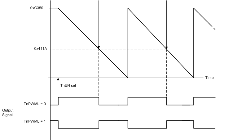
Figure 18-4 shows how to generate an output PWM with a 1-ms period and a 66% duty cycle assuming a 50-MHz input clock and TnPWML = 0 (duty cycle would be 33% for the TnPWML = 1 configuration). For this example, the start value is GPTMTnILR = 0xC350 and the match value is GPTMTnMATCHR = 0x411A.
 Figure 18-4 16-Bit PWM Mode Example
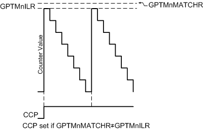
 When synchronizing the timers using the GPTMSYNC register, the timer must be properly configured to avoid glitches on the CCP outputs. Both the TnPLO and the TnMRSU bits must be set in the GPTMTnMR register. Figure 18-5 shows how the CCP output operates when the TnPLO and TnMRSU bits are set and the GPTMTnMATCHR value is greater than the GPTMTnILR value.
 Figure 18-5 CCP Output, GPTMTnMATCHR > GPTMTnILR
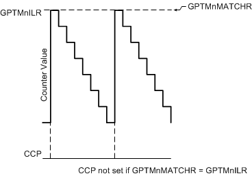
 Figure 18-6 shows how the CCP output operates when the PLO and MRSU bits are set and the GPTMTnMATCHR value is the same as the GPTMTnILR value. In this situation, if the PLO bit is 0, the CCP signal goes high when the GPTMTnILR value is loaded and the match would be essentially ignored.
 Figure 18-6 CCP Output, GPTMTnMATCHR = GPTMTnILR
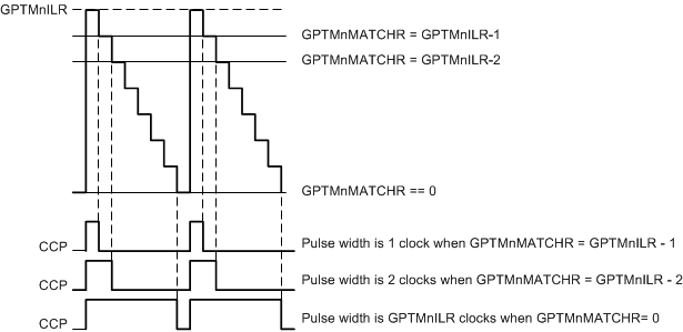
 Figure 18-7 shows how the CCP output operates when the PLO and MRSU bits are set and the GPTMTnILR is greater than the GPTMTnMATCHR value.
 Figure 18-7 CCP Output, GPTMTnILR > GPTMTnMATCHR