SLAU908B October 2023 – May 2024 MSPM0C1104
2.1 Hardware Overview
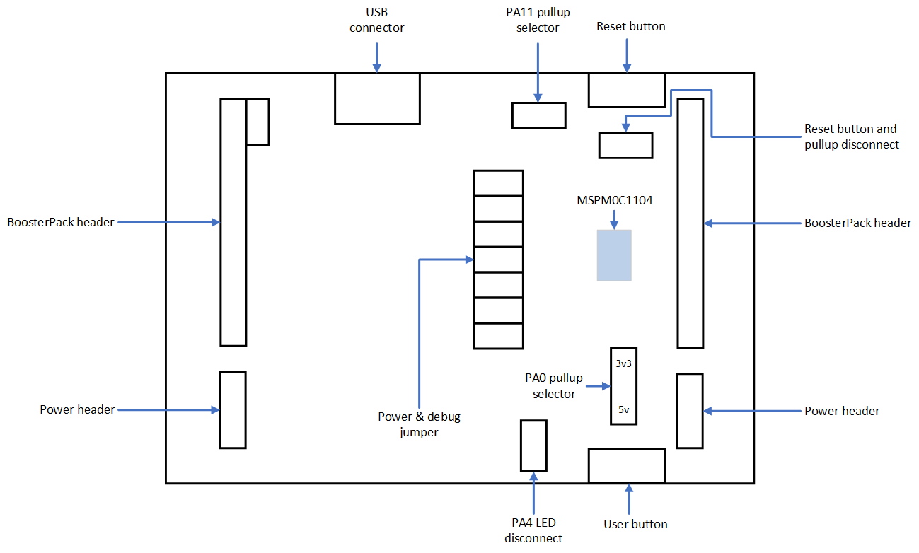
 Figure 2-1 Diagram of LP-MSPM0C1104
Jumpers and Connectors
Figure 2-1 Diagram of LP-MSPM0C1104
Jumpers and ConnectorsLP-MSPM0C1104 has many hardware features, which allow the user full access to the MSPM0C1104 pins while still providing onboard connectivity for easy use. Shunt connections provide a way for the user to easily change the LaunchPad configuration. The location of these shunts is shown in Figure 3-1. The connection of each shunt is described in Table 3-1. The default configuration is to have all shunts populated.
Table 2-1 Jumper Information
| Jumper | Description | Default Setting | Connected Signal |
|---|---|---|---|
| J6 | Pullup selection for PA0 (open drain) | Installed between center tap and 3.3V | 2.2k pullup resistor to 3.V or 5V |
| J7 | PA4(Version: E2)/PA22(Version: E3/A or other) LED connection | Installed | LED1 anode (+) |
| J8 | Pullup selection for PA11 | Installed | 2.2k pullup resistor to 3.3V |
| J9 | Reset button and pullup circuitry connection | Installed | See Section 4.1 |