SLAU917B October 2023 – February 2024 AFE20408
3.2.2.2 High Level Configuration Page
The High Level Configuration page is used to set the configuration of the AFE20408EVM GUI. The page is comprised of two tabs: DAC Control and ADC Control. These two tabs act as shortcuts to configure the AFE20408 for basic functionality and testing.
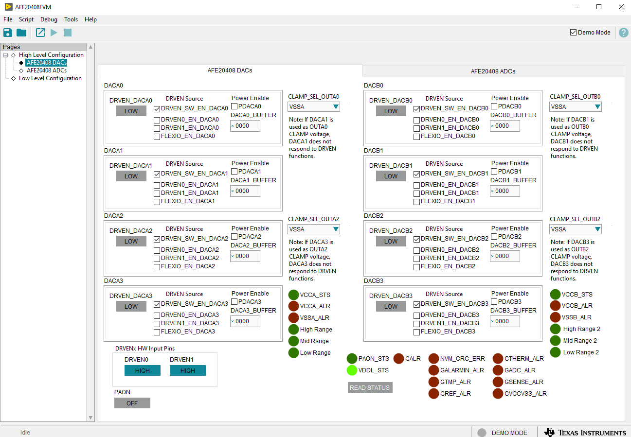
Figure 4-7 shows the DAC Control tab of the High Level Configuration page. This tab is used to set the range and outputs for the DACs. Alarms and status information is also displayed on this tab.
 Figure 3-7 DAC Control Tab of the High Level Configuration Page
DACs
DACs DACA0, DACA2, DACB0, and DACB2 are powered on by checking the respective PDACxx box. DACs DACA1, DACA3, DACB1, and DACB3 are powered on by checking the respective PDACxx box and by clicking the DRVEN_DACxx box. Write to the DAC buffers by entering hex values into the DACxx_BUFFER boxes.
DRIVE ENABLE
By default, all of the DACs are connected to the software drive enable. To enable the DRVEN hardware pins, de-select the software DRVEN and select one of the hardware DRVEN options (DRVEN0, DRVEN1, or FLEXIO). The DRVEN0 and DRVEN1 hardware pins be controlled by the GUI if jumper J23 1-2 and 3-4 are shorted.
OUT PINS
By default, OUTA0, OUTA2, OUTB0, and OUTB2 are connected to the VSSA/VSSB power supply. The CLAMP_SEL_OUTxx box sets the OUTxx pins to the respective DACxx pin. Table 4-1 shows the Output pin configurations.
| Output Pin | CLAMP Bit | CLAMP_SEL = 0 | CLAMP_SEL = 1 |
|---|---|---|---|
| OUTA0 | CLAMP_SEL_OUTA0 | VSSA | DACA1 |
| OUTA2 | CLAMP_SEL_OUTA2 | VSSA | DACA3 |
| OUTB0 | CLAMP_SEL_OUTB0 | VSSB | DACB1 |
| OUTB2 | CLAMP_SEL_OUTB2 | VSSB | DACB3 |
Furthermore, the output pins can switch between the respective CLAMP and even DACs using the even DAC's DRVEN bit. Table 4-2 shows the DRVEN configurations.
| Output Pin | DRVEN Bit | DRVEN = 0 | DRVEN = 1 |
|---|---|---|---|
| OUTA0 | DRVEN_DACA0 | DACA1/VSSA | DACA0 |
| OUTA2 | DRVEN_DACA2 | DACA3/VSSA | DACA2 |
| OUTB0 | DRVEN_DACB0 | DACB1/VSSB | DACB0 |
| OUTB2 | DRVEN_DACB2 | DACB3/VSSB | DACB2 |
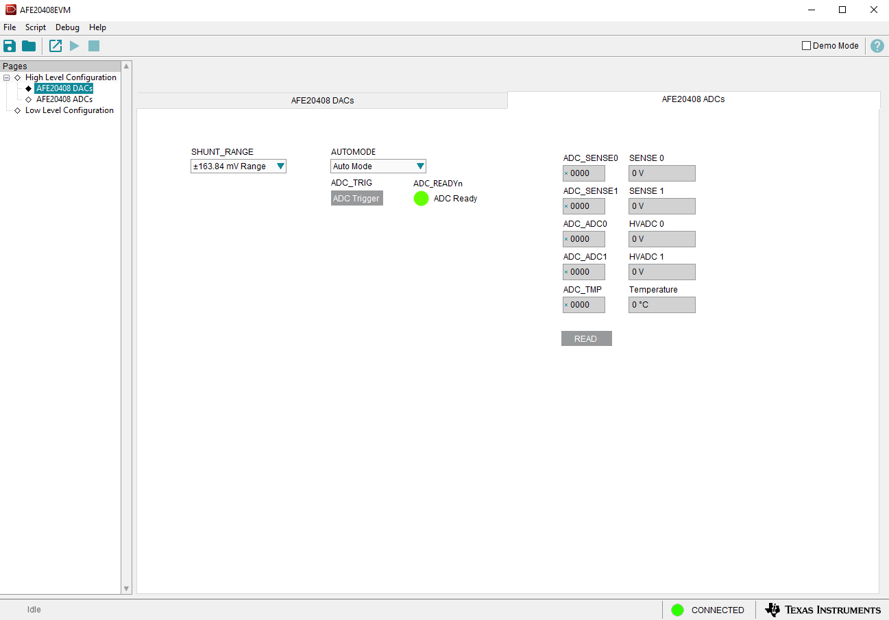
Figure 4-8 shows the ADC Control tab from the High Level Configuration page. This tab configures and reads data from the ADC in the AFE20408.
 Figure 3-8 ADC Control Tab of the High Level Configuration Page